| Schematic | PCB | Assembly | Modifications |
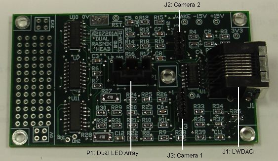
The Dual Rasnik Head (A2072) is a LWDAQ Device provides connections for two Nine-LED Arrays (A2041) and two TC237B Minimal Heads (A2070). The A2041s provide light for Rasnik masks. The A2070s hold TC237B image sensors that capture Rasnik mask images.
We define the following versions of the A2072.
| Version | Description |
|---|---|
| A | Long Guide Tube Head |
The is designed to operate with two TC237B Minmal Heads (A2070B) and two Nine-LED Array (A2041B), but it can be used with any version of the A2070 or A2041.
The A2072 is also compatible with all versions of the TC255P Minimal Head (A2016). The A2072 provides a −2.5 V bias on Pin 2 of its eight-way flex connectors. This voltage serves at the anti-blooming bias (ADG pin) for the TC255P image sensor in a A2016. The TC237B also requires a +5 V anti-blooming bias (ODB pin), but the TC237 Minimal Head (A2070) provides this bias with its own resistive divider, and does not make any connection to Pin 2 of its 8-way flex connector. The output amplifier gain of the A2072 is, however, 5.7 instead of the 2.0 that is optimal for the TC255P. The image intensity will saturate when the pixels are only partly full.
The A2072 complies with the LWDAQ Specification. When we use it to read out a TC237B, it's device type is 5 (TC237). When reading out a TC255, its device type is 2 (TC255). The image sensors are elements 1 and 2 during read jobs, and the light sources are elements 1 and 2 during flash jobs.
| DC16 | DC15 | DC14 | DC13 | DC12 | DC11 | DC10 | DC9 | DC8 | DC7 | DC6 | DC5 | DC4 | DC3 | DC2 | DC1 |
|---|---|---|---|---|---|---|---|---|---|---|---|---|---|---|---|
| X | X | X | X | X | ON2 | ON1 | CCD1 | WAKE | LB | X | X | IAGD | SAGD | SRGD | DCEN |
The signals acronyms are DCEN for direct clock enable, SRGD for serial register gate digital, SAGD for storage area gate digital, IAGD for image area gate digital, and LB for loop back. The CCD1 signal, when asserted, selects the image sensor connected to J3.
To expose the image sensor, send the following instructions to the LWDAQ driver:
To flash one of the light sources, send the following instructions to the LWDAQ driver:
You will find the above read-out sequences layed out in BCAM.tcl, the TclTk script that defines the BCAM Instrument in our LWDAQ Software.
For a discussion of image geometry, and how to translate between points in the image sensor and points in the image on our computer screen, see the Image Geometry section of the TC237B Minimal Head (A2070) Manual.
The A2072 uses the same differential transceiver, power supply switches, and logic chips as the Proximity Camera Head (A2047). For a discussion of the radiation tolerance of these components, see here. The A2072 uses some new parts, and these must be radiation tested before they enter a long-term radiation environment. We describe the component changes below.
The A2072 is a LWDAQ Device. It follows a long series of LWDAQ devices, like the A2047. We make some changes to the set of components we use in the familiar circuits, and we describe these below.
The EL2244CS is obsolete. The THS4082 is a pin-compatible replacement. It's slightly faster, but we have found it to be less robust. It is possible to damage the part by over-loading its output or over-driving its inputs. Our only experience of the EL2244CS part failing was after thousands of hours of over-heating. Furthermore, we know the EL2244CS is resistant to 100 krad and 1012 1-MeV eq. n/cm2. The A2072 schematic specifies either the EL2244CS or the THS4082, but we must test the newer part in radiation before we install it in an experiment.
The diode array MA125 is obsolete. We replace them with the BAV99DW. The new part provides two pairs of series-connected diodes for clamping and current sources. At current 330 μA, these diodes drop slightly less voltage than those of the MA125, so we find that we need seven of them in series instead of six in order to develop the 3.9-V bias voltage of our 3.3-V regulator. We discuss the temperature-dependence of these diode drops below.
The bipolar transistor array XN4501 is obsolete. We replace it with pin-compatible IMX1.
The 74LV594 is obsolete. We switched to the 74AHC594 a few years ago. The 74VHC594 is in stock at Digi-Key. Our radiation tests show no difference in radiation hardness between these families, nor is there any significant functional difference.
The A2047 and its relatives used 50-V, 1.0 μF capacitors in P1206 packages because these were the smallest we could obtain at a reasonable price in 2002. All other capacitors were in P0805 packages. The A2072 uses 50-V, 1.0 μF capacitors in P0805 packages.
Note: All our schematics and Gerber files are distributed under the GNU General Public License.
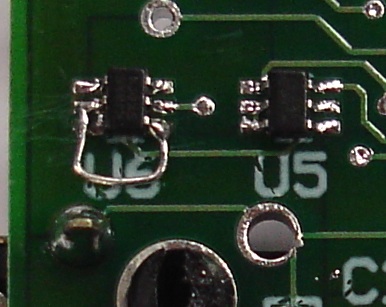
The while testing our original circuit with the A207201A we realised that our new diodes dropped too littl voltage. Our 3.3 V supply was at 2.8 V. We add another diode to the regulator biase chain in the A207201B and later, but the A207201A can be modified as shown below. First, we clip off pin U6-3 at the base. We solder U6 onto its footprint. We connect U6-2 to U6-4 with a wire link. We solder one end of the link to the U6-3 pad, and the other to the U6-4 pin.
While setting up the Long Guide Tube system at CERN in April 2011, one of the A2072As in the system started smoking. We describe the cause of this problem here.

It turns out that a shield trace on the inner layer of our A207201A printed circuit boards was connected, through a fabrication error (see here), to the 3.3-V power supply. We can isolate the short on the inner layer by snipping the shield trace in two places, as shown below.
The A2072 uses a chain of seven diodes to generate reference voltage for its logic power supply. These diodes are provided by two BAV99DW quad diode arrays (U5 and U6 in S2072_1). Although the BAV99DW is new to us, the diode-chain regulator is not. We used diode-chain regulators in almost all the devices we installed in the ATLAS cavern (see Radiation Tolerance section of the A2047 Manual). We use a diode chain regulator because it is resistant to ionizing radiation. We find it unaffected by 100 krad, and work done by other institutes suggests that the regulator should be reliable up to 300 krad.
The voltage drop across a chain of diodes is strongly dependent upon temperature, but weakly dependent upon ionizing radiation dose. Thus we might see a 10% drop in the voltage drop with a 20°C increase in temperature, and only a 1% drop in voltage with 100 krad of radiation. The temperature in experimental caverns where our alignment devices tend to be used is well-controlled to lie within 20±5°C. Thus we sacrifice operating temperature range for radiation resistance.
The voltage drop of each individual diode decreases with temperature, as shown by the following figure, taken from the data sheet. Resistors R2 and R0 allow roughly 400 μA to flow through the diodes, which is just off the bottom of the graph.
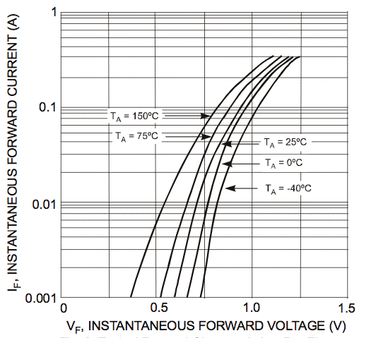
Extrapolating the graphs, we expect the 400-μA forward voltage drop to be 0.60 V at 0°C, 0.55 V 25°C, and 0.50 V at 75°C. The logic supply is seven diode drops minus the base-emitter voltage of U4, so roughly six diode drops. We expect our supply voltage to be 3.6 V at 0°C, 3.3 V at 25°C, and 3.0 V at 75°C.
We measured the 3.3-V logic supply at 18°C on five different A3022s and obtained 3.23±0.02 V. We turned on live image capture and observed the voltage varying by ±0.03 V during acquisition. We heated the board with a heat gun and the logic supply dropped to 2.8 V. We cooled it with freezer spray and it rose to 4.0 V.
The recommended supply voltage for our VHC, AHC, and LV series logic chips (such as the 74VHC123) is 2 V to 5.5 V. But our SN65LVDM180D transceiver chip requires 3.0 V to 3.6 V. Thus we expect our logic to work well from 0°C to 75°C, and probably another 20°C beyond that. We note that the supply voltage must exceed 7 V to damage the logic chips.
Although our logic circuits will function well from 0°C to 75°C, our image sensor readout may encounter its own problems. We use the logic supply voltage to determine the clock levels we supply to the image sensor. In S2072_2 we see U14 and U15 use logic signals SRG, SAG, and IAG to generate clock signals that swing between 2 V and −10 V, by amplifying the logic level voltages. As the logic supply changes, so do the clock levels. The data sheets for the TC237B, TC236P, and TC255P all specify clock voltage tolerances ±0.5 V, but we find we are able to obtain good images for deviations of at least ±1 V. Thus we are tolerant of logic supply deviations from 3.3 V of at least ±0.3 V, and therefore tolerant of temperature variation of 0°C to 75°C.
By combining the Schockley equation with an approximate relation between saturation current and temperature, we can obtain a theoretical estimate of the change in our diode chain voltage drop with temperature.

Applying the above analysis of our seven BAV99DW diodes, minus the similarly-behaved base-emitter drop of U4, we expect 6×2.4 mV/°C drop in the logic supply voltage, or −0.014 V/°C. Because we can tolerate a variation of ±0.3 V, this suggests a temperature range of 20±20°C.
We designed the A2072B for use with the Long Guide Tube (LGT). Four rasnik instruments monitor the shape of the tube from the inside. One A2072B mounts just inside either end of the tube. A motor turns a threaded rod that compresses a seven-meter aluminum tube so as to keep it straight when we apply a load to its center. Another motor rotates the tube, so as to correct for rotation caused by the compression. Each motor is controlled by an H-Bridge Head (A2060H). Power for both motors comes from a single 4-A, 24-V switch-mode power supply (LPS-100-24).

The motor drivers are combined with an Inclinometer Head (A2065B) to monitor the rotation of the LGT, a Wheatstone Bridge (A2057W) to monitor the strain in the threaded rod, and a Six-Way Patch Panel (A2059B). You will see the A2065B on the lower-left and the A2057W in the lower center of this end view of the LGT electronics enclosure. You will see the A2065B at the center and the A2059B on the left, with six LWDAQ cables leading to it, in this view. Four of these cables are for the A2060Hs, A2065B, and A2057W. The remaining two are for two A2072Bs at either end of the LGT.
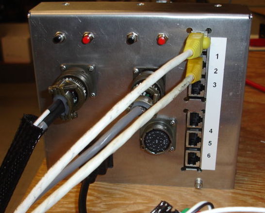
Two sets of switches allow us to drive the motors clockwise and anti-clockwise. An AC power plug accepts 120 V or 240 V. The LPS-100-24 power supply detects 110 V or 240 V and re-configures itself accordingly, so we can connect either. The six LWDAQ sockets of the Six-Way Patch Panel (A2059B) are visible on the right. Three circular connectors provide connection to three other components of the LGT. The twenty-sixe way socket on the lower-right connects to the LGT Camera Harness I, which provides connections to two A2072Bs and on Inclinometer Sensor Head (A2066). Within the enclosure, the twenty-six way socket is connected to internal circuits with the LGT Camera Harness II, leading to two A2059B sockets and the sensor input of the A2065B. The twelve-way connector on the upper-right and the four-way connector on the upper center provide connection to the A2060Hs and the A2057W. The tension rod motor and its strain gauge are connected to the twelve-way connector and the rotation motor is connected to the four-way connector. The LGT Motor Harness I provides connection from the two motor enclosures to the two plugs that mate with the sockets on the electronics enclosure.
We operated the Long Guide Tube with our LGT Tool. Run the script from the LWDAQ Tool menu.