| Schematic | PCBs | Assembly |
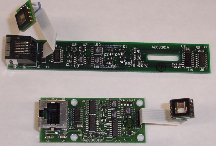
The Inplane Sensor Head (A2036) is a Long-Wire Data Acquisition (LWDAQ) Device that reads out a TC255P image sensor. Its circuit is identical to that of the Proximity Camera Head (A2033), and this manual serves as a manual for the A2033 as well. We use the A2036 and A2033 most often with the LWDAQ Software's Rasnik Instrument.

The A2036 connects to the image sensor through a flex cable and a TC255P Minimal Head (A2016). The flex cable is a 1-mm pitch, 8-way flat cable that plugs into an eight-way socket on the A2036 and the A2016. The flex cable can be up to 450 mm long. The A2016 has nothing on it except the TC255P and the flex socket. It may have an eight-way chip socket for the TC255P, so we can glue the TC255P to our image sensor chassis, and plug the A2016 onto it from behind.
The RJ-45 socket on the A2036 is a LWDAQ device socket. A LWDAQ device socket connects to a LWDAQ driver (such as the A2037) or multiplexer (such as the A2046) with a LWDAQ cable. The Proximity Camera Head (A2033) is a long, thin version of the A2036, with a slot for a screwdriver to pass through to a mounting screw below.
The A2036 is complies with the LWDAQ Specification. It is Device Type 2 for the purpose of device-dependent jobs. It ignores the Device Element number.
| DC16 | DC15 | DC14 | DC13 | DC12 | DC11 | DC10 | DC9 | DC8 | DC7 | DC6 | DC5 | DC4 | DC3 | DC2 | DC1 |
|---|---|---|---|---|---|---|---|---|---|---|---|---|---|---|---|
| X | X | X | X | X | X | X | X | WAKE | LB | ABEN | ABGD | IAGD | SAGD | SRGD | DCEN |
The A2047 does not provide anti-blooming.
The A2036 provides exposure of the TC255P with no anti-blooming. Anti-blooming is good for pictures that give us the rough location of features, but it compromises the linearity of the pixel response, and is therefore detrimental to the performance of survey cameras. The A2036 is asleep when it powers up, and goes to sleep when you execute a sleep job.
Consider an A2036 fastened next to a TC255P on a structure whose distortions we wish to monitor. A lens some distance away focuses an image of a reference pattern upon the TC255P's imaging area. The reference pattern is illuminated by an Inplane Mask Head (A2052). We would like to take images as fast as we can. Our LWDAQ Driver is an A2037, and it is 80 m away.
We connect the A2036 to the TC255P. We choose a version of the TC255P Minimal Head (A2016) that fits on the back of our TC255P, and allows us to plug in an 8-way flex cable and run the cable to the sensor head. We plug the flex cable into the A2036. If we plug it in the wrong way, we won't get images, but we won't damage the TC255P either. We have to get it the right way round eventually, but there is no need to be careful about it.
We connect the A2036 and the A2052 to the LWDAQ Driver with two 80-m cables. We can read out two million image pixels per second from the TC255P. We do not gain by making the cables shorter.
We start up our DAQ software and run a loop job for both devices to check that they are connected and responding. The loop-back timer in the driver should read something close to thirty-two. Its counting frequency is 40 MHz, so thirty-two is 800 ns, or 400 ns each way on the cable. The propagation delay down CAT-5 cable is approximately 5 ns/m.
We capture an image. With our LWDAQ Driver, we execute upon the A2036 a move job, which clears the image sensor, and a wake job, which puts leaves the image sensor to gather light. We run a flash job on the A2052, clear the driver's address counter, run an alt move job to move the image into the storage area, and a read job on the A2036 to bring the image into the driver memory. We transfer the image from the driver's memory to our computer memory and display it on the screen. We repeat the process for the next image. We might get five images a second this way, assuming the exposure time is a matter of milliseconds. One of the slowest parts of the process is importing the image from the driver into the computer, and displaying it. We can speed things up by displaying the image while the next one is being transferred from the TC255P into the driver. This might raise our display rate to ten images per second.
Our DAQ code may make a habit of running a sleep job on the A2036 after every read job. If so, then the A2036 will dissipate less than 15 mW when it is idle. Otherwise, it will dissipate as much as 500 mW.
As you can see from the above example, we expose the TC255P with a sequence of LWDAQ Driver jobs: move, wake, flash, alt_move, and read. This sequence ends with the eight-bit gray-scale image in the driver memory. For a more detailed description of the read-out sequence, see the Operation Section of the A2051 Manual. The A2051 readout is identical to that of the A2036, except that the A2036 does not support anti-blooming, while the A2051 does. You will find the full sequence of data acquisition steps defined in Rasnik.tcl, which is the TclTk script that defines our LWDAQ Software's Rasnik Instrument. To see how we compose TCPIP messages for communication with a LWDAQ Driver, see Driver.tcl.
Once we are capturing images, we need to adjust the exposure time until we get the image we want. If the exposure time is too long, the image will be white. If it is too short, it will be black. The black image from a working A2036 is, however, different from the black image from a broken A2036, or one that is not connected. Each driver introduces its own noise, but this will be less than the noise present in the black image from a working head.
We will most likely need to determine which side of the TC255P corresponds to which side of the image on our screen. We determine the orientation by experiment. Each A2016 has its own orientation, the driver reads the image according to the design of the TC255P, and our software can flip the image up and down as well. By the time we are through figuring out all these rotations, it will have been quicker determine the answer directly.
We picked an A2036 at random and measured its power consumption in three states.
| State | +15 V | -15 V | +5 V | Total Power |
| Asleep | 10 μA | 10 μA | 2.6 mA | 13 mW |
| Awake (0 images/s) | 36 mA | 36 mA | 4.0 mA | 1.1 W |
| Awake (6 images/s) | 38 mA | 38 mA | 4.5 mA | 1.2 W |
The A2036 proved to be vulnerable to ionizing radiation. Samples of the obsolete A2033 assembly, whose circuit is identical to that of the A2036, irradiated under +5 V power but without ±15 V power, operated normally after 20 krad plus four-week room-temperature anneal, but failed after 100 krad plus four-week room-temperature anneal. There were three causes of failure. First, the output voltage of the MAX6329 regulator (see schematic) rose by about 0.2 V at 20 krad and 1 V at 100 krad. Second, one of the DG411 switches (see schematic) was stuck open after 100 krad. Thirdly, one of the 74VHC123A monostable flip-flops (see schematic) was refusing to fire after 100 krad.
Later tests with power applied to the circuit, and radiation at 20 krad/hr showed three out of three fully-powered A2036s failing after 30 krad plus four-week room-temperature anneal, and for the same reasons. Current passing into the boards began to spike at around 20 krad. We estimate the ionizing radiation resistance of the A2036 at around 20 krad. We also suspect that damage occured to the circuits during irradiation due to excessive power consumption caused by temporary radiation effects in the circuits.
The A2047 is a radiation-hardened descendent of the A2036. It is functionally equivalent, but replaces the MAX6329 with a transistor-diode regulator, and the DG411 with discrete MOSFETs. The 74VHC123 remains, but with its power supply stabilized, it proves to be more resistant to radiation. The A2047 command receiver circuit, containing the 74VHC123, appeared to be unaffected by 30 krad of ionizing radiation, although the 74VHC123 failed at 100 krad.
For a discussion of image geometry, and how to translate between points in the image sensor and points in the image on our computer screen, see the Image Geometry section of the TC255P Minimal Head (A2016) Manual. For instructions on finding Pin One on a TC255P, see the Pin One section of the same manual.
The A2036 has two zener diodes, Z2 and Z3, clamping the analog return lines to 0 V, as shown here. These zener diodes protect the LVDS transceiver from the pixel amplifier op-amp U4. We overlooked the fact that these zener diodes would load the R± lines with approximately 200 pF. This reduces the returned differential amplitude for both analog (pixel) and digital (loop-back) data. As if that was not bad enough, the LVDS transceiver has a design error (acknowledged by Texas Instruments after they received our report) by which the LVDS chip does not enter its high-impedance state properly. Instead, the chip loads the return lines with a non-linear impedance that further attenuates the returned signal amplitude, and distorts its shape. These two problems reduce A2036's saturated image contrast. The reduction is small for short cable lengths, but becomes significant for longer cables.
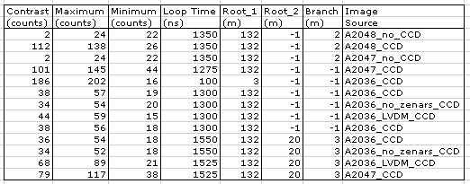
 Table: Image Contrast, in eight-bit ADC counts for various image sensor heads and various modifications to the A2036.
The figure above shows the saturated image contrast we obtain from various TC255 image sensor heads with the CCD exposed to overhead lighting. The final four lines in the table show the contast we obtain with a 132-m root cable leading to a repeater, then 20 m more cable to a multiplexer, and then a final 3 m to the image sensor circuit. The A2047T is a revised version of the A2036. Instead of an SN65LVDS180D chip, it has the pin-compatible SN65LVDM180D, which enters its high-impedance state correctly. Its analog output stage has no zener diodes, and operates through 100-Ω resistors, as you can see in the here. The A2047 returns an image contrast of 79 counts across the total 155 m of cable. But an unmodified A2036A returns only 36 counts. If we replace the A2036A's LVDS chips with an LVDM chips, the contrast increases to 68 counts. If we remove the zener diodes instead, we get hardly any improvement.
Replacing the LVDS chip with the LVDM almost doubles the A2036's image contrast over long cables. Removing the zener diodes makes hardly any difference. But even without these modifications, the A2036's image contrast should still be adequate for the A2036's intended purpose. An image with contrast 10 counts and noise less than 1 count rms is perfectly adequate for a Rasnik Instrument.
The Inplane Sensor Head (A2047) is functionally equivalent to the A2036, but offers greater resistance to radiation and greater image contrast. The A2047 drives the analog return lines through resitors that provide fast, bounce-free differential drive of the analog return lines, as shown here. The following table lists each of our TC255P sensor readout circuits and classifies them according to whether they have the A2047 or the A2036 analog return circuit.
| Circuit | Analog Return Type |
|---|---|
| Proximity Camera Head (A2033) | A2036 |
| Inplane Sensor Head (A2036) | A2036 |
| BCAM Head (A2038) | A2036 |
| Proximity Camera Head (A2047) | A2047 |
| Azimuthal BCAM Head (A2048) | A2047 |
| Polar BCAM Head (A2051) | A2047 |
| Camera Head (A2056) | A2047 |
The Camera Head (A2056) provides anti-blooming, which compromises the linearity of the TC255P response but stops pixels from over-flowing into neighboring pixels, so that we don't get big smears of white around bright lights in the image.
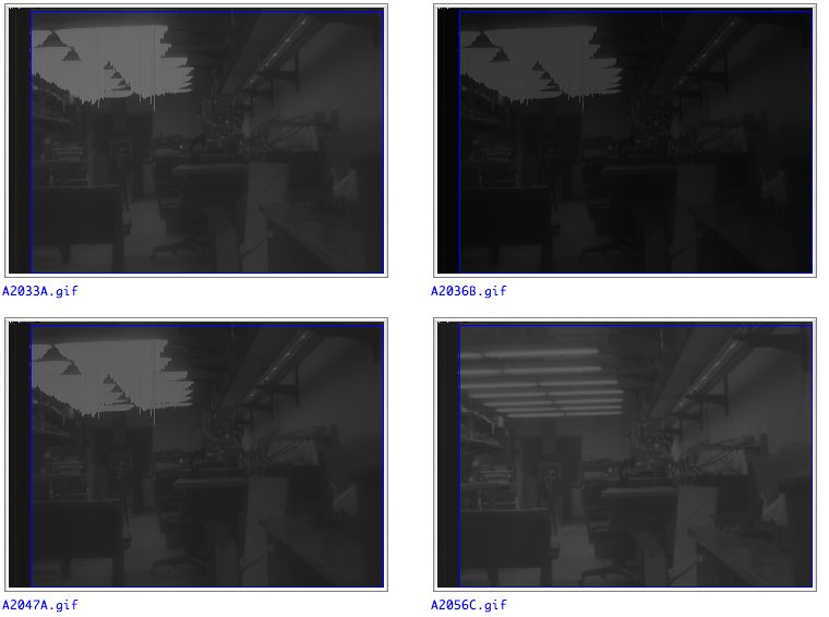
The figure below shows images taken from various TC255P circuits with an 80-m root cable. The images are not intensified, so you can see how dim they are as a result of traveling along the cable, or due to the poor gain of the analog return circuit.

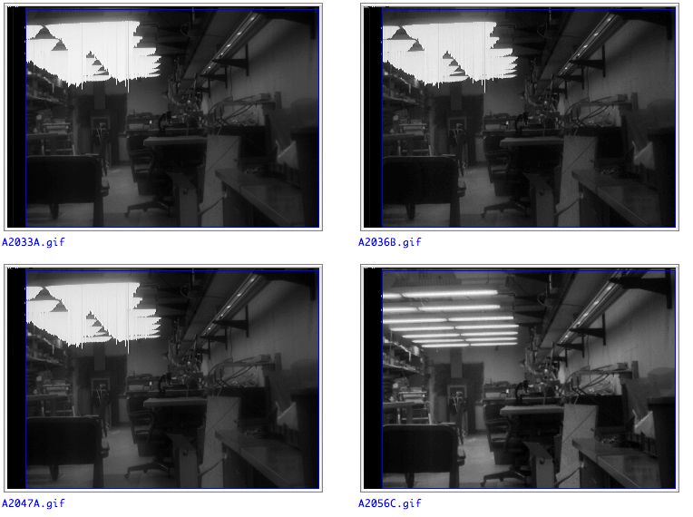
Here are the same images, but this time with intensification.

[13-MAY-09] We made roughly 1,400 A2036s for the ATLAS experiment, starting in 2001. We used one or two hundred of them in a series of test stands. The first 10% of them we made by hand. The remaining 90% were made by machine. We tested all the circuits before we installed them. If any of the hand-made circuits failed to work, we fixed them. But when a machine-made circuit failed we set it aside. Over the years, we accumulated twenty or thirty faulty machine-made circuits. At times, we tested and fixed the faulty circuits. Half the time, we found that C6, a 10-nF capacitor, was cracked. The remaining problems were vairous: pins with not enough solder, wrong resistor values, and cracked resistors.
In May 2009, we received seventeen A2036 circuits back from CERN. Some were hand-made A2036As retrieved from test stands. Others were machine-made A2036Bs. All were in a single box at CERN. It is possible that some of the boards were placed in the box because they were faulty. All the circuits returned to us were giving bad images at CERN, often with horizontal strips and no horizontal definition, and sometimes with vertical smearing of rasnik features.
We took each circuit, gave it a number, plugged it in, analyzed its current consumption with the Analyzer Tool, waited 60 s, inspected, tested it with a camera, cooled with compressed air, tested with camera, heated with a heat gun, tested with camera, checked capacitor C6 to see if it is cracked, and inspected the RJ-45 socket springs. We record all observations below.
| Number | Analyzer | Inspection | Image Cool |
Image Cold |
Image Hot |
C6 | Springs |
|---|---|---|---|---|---|---|---|
| 1 | Correct | Rosin flux residue. | Perfect | Perfect | Perfect | Okay | Okay |
| 2 B | Bad Currents | U8 hot when asleep. −15 V stays on. |
Rare Inverted | Perfect | Perfect | Okay | Okay |
| 3 | Correct | Perfect | Perfect | Perfect | Perfect | Okay | Okay |
| 4 B | Bad Currents | U8 hot when asleep. −15 V stays on. |
Usually Inverted | Inverted | Usually Perfect | Okay | Okay |
| 5 B | Bad Currents | U8 hot when asleep. −15 V stays on. |
Inverted | Usually Inverted Sometimes Black |
Usually Perfect | Okay | Okay |
| 6 B | Bad Currents | −15 V stays on. | Noise Only | Noise Only | Noise Only | Okay | Okay |
| 7 B | Bad Currents | −15 V stays on. | Noise Only | Noise Only | Noise Only | Okay | Okay |
| 8 B | Bad Currents | U8 hot when asleep. −15 V stays on. |
Partially Inverted | Perfect | Inverted or Black | Okay | Okay |
| 9 B | Bad Currents | U8 hot when asleep. −15 V stays on. |
Sometimes Inverted | Corrupted | Corrupted | Okay | Okay |
| 10 B | Bad Currents | U8 hot when asleep. −15 V stays on. |
Usually Perfect | Corrupted and Noisy | Perfect | Okay | Okay |
| 11 | Bad Currents | U8 hot when asleep. −15 V stays on. |
Corrupted | Inverted | Corrupted | Okay | Okay |
| 12 | Bad Currents | U8 hot when asleep. −15 V stays on. |
Corrupted | Corrupted | Perfect | Okay | Okay |
| 13 | Correct | Perfect | Perfect | Perfect | Perfect | Okay | Okay |
| 14 | Bad Currents | U8 hot when asleep. −15 V stays on. |
Perfect | Perfect | Minor Corruption | Okay | Okay |
| 15 | Correct | Perfect | Perfect | Perfect | Perfect | Okay | Okay |
| 16 | Correct | Perfect | Perfect | Perfect | Perfect | Okay | Okay |
| 17 | Correct | Perfect | Noise Only | Noise Only | Noise Only | Okay | Okay |
| 14 New U11 | Correct | Perfect | Perfect | Perfect | Perfect | Okay | Okay |
| 17 New U8 | Bad Currents | Perfect | Perfect | Perfect | Perfect | Okay | Okay |
As you can see, many of the boards had the same problem: the −15V supply to the analog circuits was failing to turn off when the board went to sleep. As a result, op-amp U8 was over-heating. This device is a dual op-amp, the EL2244CS. We replaced the DG411DY analog switch, U11, in No14 and the board functioned perfectly afterwards. These switches were made by Siliconix. We have never had any trouble with Siliconix switches before, but we have had problems with switches made by other manufacturers.
An A2036B with a faulty U11 would over-heat U8 while the board was asleep. An image-capture test would show no problem at first, but as days went by, U8 would begin to suffer damage. Ultimately, U8 would fail completely, and draw no more current. Circuit No17 is an example of the complete failure of U8. The surface of U8 was discolored. We replaced U8 on No17 and obtained perfect images from it afterwards, even though U11 was still faulty.
We conclude that testing with the Analyzer Tool is necessary to confirm the functionality of an A2036, in addition to our traditional image-capture test.
[04-JUN-09] We loaded connectors into 40 pre-assembled A2036 circuits and tested all of them with the Analyzer. Thirty-nine passed the test. One showed 10 mA extra consumption from ±15V, but did not exhibit the broken analog switch problem.
Note: All our schematics and Gerber files are distributed for free under the GNU General Public License.