The TC255P Minimal Head (A2016) holds an TC255P image sensor and provides a connector through which the sensor may be controlled and read out. The TC255P is a CCD (charge-coupled device) in a 0.4" wide 8-pin DIP package. The TC255 (no P) is the same sensor in a 0.3" wide 8-pin ceramic DIP package. The A2016S accommodates the TC255's narrower package. The TC255P is a frame store CCD. The sensor consists of an image area and a storage area. The image area is exposed to light. It contains 244 rows and 344 columns of 10-μm square pixels. The storage area is in darkness. We acquire an image in the image area, move it into the storage area row by row, and read it out from the storage area pixel by pixel.
We power the sensor with +12V. We control it with clock signals that switch between +2V and −11V. The sensor produces a series of pixel intensities in the form of an analog voltage that varies between roughly 10V for black and 9V for white. The connector provided by the A2016 is an eight-way 1-mm pitch flex connector for use with an 8-way 1-mm pitch flex cable. Inside an aluminum enclosure, we notice no degradation of image quality for flex cables up to 15 cm, and we are able to acquire images with 45-cm flex cables, which are the longest we have been able to buy. A 45-cm flex cable picks up enough noise that we see diagonal shading in the image.
We chose the pin-out of the eight-way flex connector so that plugging the flex cable in the wrong way around would cause no damage to either the TC255P or the control electronics.
The A2016 comes in many varieties, some of which we show in pictures below. Each connects to a larger circuit board from which it obtains power and clock signals, and to which it delivers the image pixels. The A2016 gives the image sensor mechanical isolation from the larger circuit that drives it, and therefore from the larger circuit's external power cable.
You may connect any of the A2016 minimal heads to any of our series of control circuits that provide an eight-way flex socket for a TC255P. Examples are the Inplane Sensor Head (A2036), Bar Head (A2044), Azimuthal BCAM Head (A2048), Proximity Camera Head (A2047), and Camera Head (A2056). All these control circuits are examples of LWDAQ (Long-Wire Data Acquisition) devices. We use them to obtain images with the help of a LWDAQ driver and our LWDAQ Software. For an introduction to the LWDAQ, see the LWDAQ User Manual.
Determining Pin 1 on a TC255P package can be difficult. The markings on the package have changed over the years, and can be misleading. For a photograph of a TC255 showing the bond wires, see below. The only reliable way to find Pin 1 is to look through the glass and find the bond wires that connect the sensor's storage area to its pins. The image area is the rectangle above the rectangle with the bond wires. Pin 1 is the top-left pin when you hold the sensor with the storage area towards the bottom. Do not use the color of the image and storage areas as a clue to which is which. Use the bond wires. We once soldered 160 TC255Ps upside-down into A201601Ls because we believed the image area was the darker rectangle. But our new batch of TC255Ps had a dark storage area and a light-gray image area. The bond wires, however, are always on the storage area, and will always show you where Pin 1 is on the sensor. For a detailed drawing of the TC255P package, see here.
The following versions of the TC255P Minimal Head (A2016) exist. We describe each version by giving the location of the flex connector, J1, with respect to the image sensor. To define our directions: up, down, left, right, top, bottom, we look straight down at the image sensor, with Pin 1 of the package on the top-left. The top side of the PCB (printed circuit board) is the side upon which the image sensor is mounted. The bottom side is the other side of the PCB. The directions up, down, left, and right lie in the plane of the PCB. When we say the connector is oriented vertically, we mean the length of the connector is in the up-down direction. Horizontal (H) orientation puts the length of the connector in the left-right direction. Pin 1 of the flex connector might be marked on the top of bottom silk screen with a small 1 numeral, or it might not be so marked. But Pin 1 will always be distinguished from the other eight pins of the flex connector footprint by its square pad shape. Similarly, Pin 1 of the image sensor socket is square.
| Version | J1 Location and Orientation |
| A | bottom-side, horizontal, pin-1 left, above sensor |
| B | top-side, horizontal, pin-1 right, below sensor |
| C | bottom-side, vertical, pin-1 down, centered on sensor |
| D | bottom-side, horizontal, pin-1 right, below sensor |
| E | bottom-side, vertical, pin-1 top, left of sensor, mounting holes |
| L | top-side, horizontal, pin-1 left, below sensor, mounting holes |
| P | bottom-side, vertical, pin-1 down, centered on sensor, reduced-size A2016C |
| R | top-side, horizontal, pin-1 left, below sensor, mounting holes |
| S | bottom-side, vertical, pin-1 down, centered on sensor, for 0.3" DIP-8 |
On each version, the image sensor may be soldered directly to the board or plugged into a socket. Here are the A2016 assemblies, showing the flex connector orientation. To get an idea of the size of the heads, compare them to the 0.1-inch (2.5-mm) pitch of the pins on the sensor, or the 0.4-inch separation of the two rows. The flex cable conductors are on a 1-mm pitch.


Here we present image coordinates and show how we translate between coordinates in an image on our computer screen to coordinates in the plane of an image sensor. Our discussion is not particular to the TC255P that mounts on the A2016, although we use the TC255P as our most prominent example of an image sensor.
The TC255P provides 243 rows of 324 light-sensitive pixels. Each pixel is 10 μm square. All LWDAQ drivers and TC255P devices acquire images from the TC255P in the same way. They create an image with 244 rows and 344 colums. The rows are numbered 0 to 243 and the columns are numbered 0 to 343. The top row is generated by the data acquisition syste, and used by the data acquisition software to store the image dimensions, its analysis boundaries, and other particulars of data acquisition, as we explain in Image Files. The remaining 243 rows contain pixels from the TC255P image area. In each row, there are 324 light-sensitive pixels from the image area. These are the right-most 324 pixels. The first 6 pixels are dummy pixels generated by the LWDAQ driver. The next 2 pixels are dummy pixels generated in the TC255P. The next 12 pixels are black-level pixels from the image area. They are pixels covered by opaque aluminum. Thus all TC255P images obtained with the LWDAQ will have a black stripe 20 pixels wide on the left side.
If you hold the TC255P up so that pin one is on the top-left, you will see the image area as the top rectangle under the window. The LWDAQ reads out the bottom-left pixel in the image area first, and proceeds along the bottom row to the right. When it has read out the bottom row, it starts with the next row up, beginning with its left-most pixel. The last pixel the LWDAQ reads out is the top-left pixel in the image area.
The result of data acquisition from the TC255P is a gray-scale image. The LWDAQ software will display the image on our screen. All LWDAQ image analysis routines agree upon the definition of image coordinates, which we use to define points in the image and on the sensor. The image coordinate origin is the top-left corner of the top-left pixel in the image as it appears on our computer screen. But the top-left pixel in the image is the bottom-left pixel in the light-sensitive area on the sensor. The figure below attempts to show how image coordinates appear on the sensor and in the display.

As you can see, image coordinates are right-handed on the sensor but left-handed in the image we create with our software. Suppose we place a lens in front of the image sensor and focus an image of an object upon the sensor surface. The image on the sensor is an inverted mirror-image of the object. But as we go from the sensor to the computer screen, we invert and reflect the image so that what we see on the screen is an upright and unreflected image of the object.
The way we remember our definition of image coordinates is as follows. We remember our definition of upright for our image sensor. In the case of the TC255P, the sensor is upright when the long side of its package is vertical and Pin 1 uppermost. We figure out simple optics that the image of an object on the sensor must be inverted and reflected. We remember that the image we obtain from a camera with an upright image sensor will be upright and unreflected. Now we draw pictures and arrive at a sketch like the one above.
Our image coodrinate origin is at the top-left corner of the top-left pixel in the screen image. This top-left pixel is not a pixel from the sensor. Indeed, the top row of any LWDAQ-generated image will be a dummy row used to store image meta-data. The fact that our origin pixel is not taken from the set of light-sensitive pixels does not detract from the value of our definition. The top-left edge of the top-left pixel is a definition that we can apply without ambiguity to any image, regardless of its dimensions or the size of its pixels. The TC255P pixels are 10 μm square and TC237B pixels are 7.4 μm square. A TC255P image sensor provides 243 rows of 324 active pixels. A TC237 provides 496 rows of 658 active pixels.
Our spot-finding routines are defined in spot.pas. We use these routines in many instruments. We use them to find light spots in BCAM images. We use them to find wire silhouettes in WPS images. The routines determine the location of features in image coordinates. Our routines assume that all pixels are square, and they require that we specify the pixel width in microns. They return the position of features in microns from the origin of image coordinates as it appears on the sensor, with x and y defined as in the figure above. When a feature has an orientation, as does a wire silhouette, our routines specify the rotation in milliradians, with positive rotation when the feature rotates anti-clockwise with respect to the image.
When we are measuring the location of an large feature, such as a Rasnik Mask or a Stretched Wire, we tend to use the center of the image as a reference point for the measurement rather than the origin of image coordinates. Using the center of the image reduces the effect of errors in our rotation measurement upon our measurement of position. In TC255P images, our routines use the top-left edge of pixel 172 in the row 122 as the center. In units of pixels, the center is (172, 122). The TC255P has 10-micron square pixels, so in units of microns the center is at (1720, 1220). In units of millimeters, the center is at (1.720, 1.220). The following definition is from bcam.pas.
const
	bcam_ccd_center_x=1.720;{along ccd x-axis (mm)}
	bcam_ccd_center_y=1.220;{along ccd y-axis (mm)}
The Rasnik Instrument allows us to specify a variety of reference points. We can choose the origin of image coordinates, the default center of the image, or we can provide our own reference point in image coordinates with analysis_reference_x_um and analysis_reference_y_um. We specify the reference point in microns. We also specify the image pixel width and height with the single parameter analysis_pixel_size_um.
The WPS Instrument allows us to specify a reference y-coordinate at which we will determine the x-coordinate of the center of a wire silhouette. We specify the y-coordinate in microns with analysis_reference_um.
For a more detailed drawing of the TC255P package, which gives the location of the center of the image area with respect to the pins and package corners, see the package drawing.
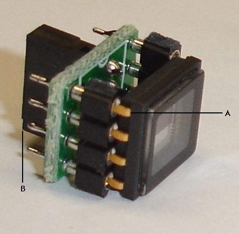
You may wish to glue the sensor to a post, and attach the A2016 from behind with a socket. This is what we did in our Proximity Cameras, as shown below. In this case, we found that we had to solder the CCD into the socket to make it secure.

When you solder the CCD into a socket, you do so one pin at a time. You heat the socket and pin together, and apply solder. You should see the solder flow down into the socket, giving you a shiny concave joint, as shown in the photograph above. Applying heat to the first pin can be tricky, because there is no other soldered pin holding the socket to the CCD. It's easy to push too hard on the iron and push the socket off.
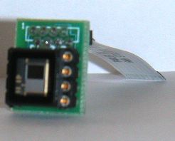
Example: We glue the sensor into a cradle in an image sensor assembly, then solder the A2016C onto the sensor from behind. The flex connector is already soldered onto the circuit board. We connect the A2016 to an Inplane Sensor Head (A2036) with a six-inch flex cable. We connect the A2036 to a LWDAQ Driver (A2037), and retrieve images from the A2016 through the A2036. We transfer these images over the Internet and display them on our computer screen with the help of the LWDAQ Software.
We have tested the A2016 with flex cables up to 45-cm long. As the cable gets longer, electronic noise degrades the image. We notice no degradation of image quality for cables less than 10 cm.
The TC255 comes in two versions: TC255P and TC255. The TC255P comes in a 10.16-mm (0.4-in) wide plastic eight-pin DIP package. The TC255 comes in a 7.62-mm (0.3-in) wide ceramic eight-pin DIP package.

We cannot find a drawing of the ceramic package on the web, so we measured a TC255 ourselves and produced this drawing. The TC255 is electrically compatible with the TC255P. We can mount a TC255 in the place of a TC255P using the instructions given here. The method we describe places the image area of the TC255 in the same location as that of a TC255P, if the plastic version were soldered into its footprint. The method may be used whenever we are soldering the image sensor directly into a circuit board, which is rarely the case with the A2016. We used the TC255 in roughly one hundred BCAMs, but these do not use the A2016 to hold their image sensors. We compare the TC255P and TC255 dark current and bright pixel intensity below.
The following table gives the dark current accumulation after one second at 21°C in ten TC255P sensors we selected at random from our available inventory in 2011. To obtain the dark current, we expose in darkness for one second and subtract the black-level voltage we obtain from the leftmost five columns.
| Sensor | Dark Current | Brightest Point |
|---|---|---|
| 1 | 69.8 | 162 |
| 2 | 84.3 | 166 |
| 3 | 66.2 | 103 |
| 4 | 72.4 | 110 |
| 5 | 60.2 | 177 |
| 6 | 71.3 | 170 |
| 7 | 81.3 | 115 |
| 8 | 60.6 | 142 |
| 9 | 61.7 | 182 |
| 10 | 66.1 | 112 |
| ave | 69.4 | 143.9 |
| max | 84.3 | 182.0 |
When the pixels saturate, their intensity is around 250 counts, of which 50 is black-level, so the pixels can accomodate 200 counts of dark current before they saturate. The average TC255P will fill up with dark current in around 3 s, but some will fill up in 2.5 s. The number and intensity of bright pixels varies from one sensor to the next. We discuss the effect of radiation upon the dark current below.
The following table presents the same dark current measurement for a batch of TC255s we received in 2011.
| Sensor | Dark Current | Brightest Point |
|---|---|---|
| 1 | 53.6 | 121 |
| 2 | 51.8 | 121 |
| 3 | 52.8 | 114 |
| 4 | 46.1 | 118 |
| 5 | 65.3 | 126 |
| 6 | 57.7 | 111 |
| 7 | 56.8 | 113 |
| 8 | 62.8 | 123 |
| 9 | 58.5 | 130 |
| 10 | 56.7 | 131 |
| ave | 56.2 | 121.8 |
| max | 65.3 | 131.0 |
These TC255s have slightly lower dark current than our TC255Ps, and slightly lower bright spot intensity as well. But to the first approximation, the two versions are equivalent.
The TC255P is a member of a family of CCDs designed by a collaboration between the Jet Propulsion Laboratory and Texas Instruments. The CCDs are designed to be resistant to ionizing radiation. We tested the TC255P in neutron radiation twice. We report on our 1998 test in here and our 1999 test here. We summarize the results of ionizing and neutron radiation tests in Pre-Production Radiation Tests. Our ionizing tests indicate that the TC255P can tolerate over 1 Mrad when used with the LWDAQ. Neutron radiation increases the TC255P dark current. After 1012 1-MeV eq. n/cm2, the dark current at room temperature will fill up the pixels in only 400 ms, as compared to roughly 4 s for an un-damaged CCD. By keeping our exposure times below 40 ms, we can tolerate such a dark current, and so the TC255Ps in the ATLAS detector can tolerate 1012 1-MeV eq. n/cm2, which is over ten times the maximum dose we expect at full luminosity for ten years.
Note: All our schematics and Gerber files are distributed for free under the GNU General Public License.
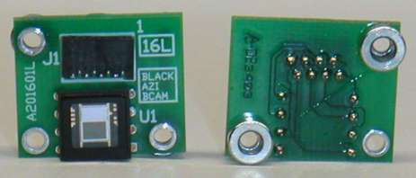
There are no components on the A2016 other than the sensor and connector. Socket J1 is a 1-mm flex cable socket. We buy ours from Digikey. Some sockets have contacts on one side, others have contacts on both sides. The table below gives the TC255P connections present on the pins of the eight-way socket.
| Signal | J1 Pin | U1 Pin | Full Name |
| OUT | 3 | 4 | output |
| SAG | 4 | 6 | storage area gate |
| SRG | 8 | 5 | serial register gate |
| ABG | 2 | 8 | anti-blooming gate |
| +12V | 1 | 2 | drain voltage supply |
| 0V | 5 | 3 | substrate voltage supply |
| IAG | 6 | 1,7 | image area gates |
The sensor (U1) can be soldered directly onto the printed circuit board, or inserted in a socket made out of two 4-way SIL (single-in-line) sockets. We have been unable to find 0.4-inch DIP sockets for the TC255P, so we make our own out of SIL sockets.
The TC255 data sheet shows how we use the clock voltages to read the image out of the CCD. The entire sensor is a shift register, where we can shift all pixels down one row by applying a pulse to the IAG and SAG clocks at the same time. Both pins rests at −11 V by default. The pulse takes both signals to +2 V. The image area acquires the image and the storage area holds the image while we read it out pixel by pixel. Moving the rows out of the image area is fast, but reading the individual pixels out is slow. We read out each pixel with a negative pulse on SRG. When SRG is +2V, the CCD output voltage corresponds to the black level. When SRG is −11 V, a new pixel intensity appears at the output, in the form of a voltage drop from the black leve.
The IAG clock moves rows in the image area down towards the storage area. The SAG clock moves rows in the storage area down into the output serial register. The SRG clock moves the pixels out of the output serial register to the output pin. To clear the CCD of charge, we apply a thousand or so pulses to the IAG and SAG clocks at the same time. All charge in both areas is moved through the output serial register and dumped into the substrate. To acquire an image we wait while the image forms in the image area. We move the image into the storage area by clocking the IAG and SAG lines 244 times. We read out the image by clocking one line at a time into the output serial register.
The LWDAQ digitizes each pixel by measuring the difference between the black level and the pixel light level. The LWDAQ read_job for the TC255 device drives SRG high for 375 ns, which gives the LWDAQ Driver time to clamp to the black level, and low for 125 ns, which gives the driver a clear 50-ns window in which to sample and digitize the difference between the two.
Page 1: TC255 SocketHere are the available printed circuit board layouts.
A201601: All versions Traxmaker files.