 Patch Panel (A2059) Manual
© 2004, Mike Bradshaw, Brandeis University.© 2006-2009, Kevan Hashemi, Brandeis University.
| Common 0-V | Broken Shield | Bad Channels |
The Patch Panel (A2059) combines six LWDAQ Repeaters (A2058) on one circuit board.
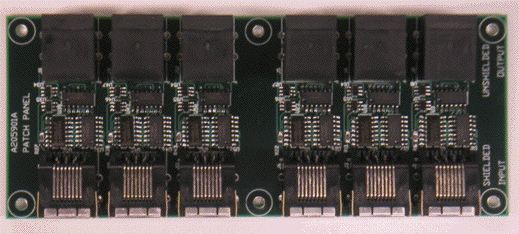
A single A2059A in an enclosure makes a Six-Way Patch Panel. For a drawing of the enclosure, showing the locations of its mounting holes, see here.

Two A2059As in an enclosure make a Twelve-Way Patch Panel. For a drawing of the enclosure, showing the locations of its mounting holes, see here.

The following versions of the A2059 exist.
| Version | Description |
| A | Patch Panel (improper shielding, 10% bad channels) |
| B | Patch Panel (proper shielding, no bad channels, red dot on chassis) |
The A2059A has a number of problems. The A2059B solves two out of three of these problems. It provides proper shielding, and eliminates the A2059A's bad-channel problem. We mark a patch panel containing A2059B electronics with a red dot on the top side.
See the A2058 Manual for links to documents that describe how to operate the A2059 with LWDAQ Hardware.
The A2059A shares the same problems as the A2058A, as listed here. In addition, it has the following problems.
The repeaters on the A2059A were supposed to be entirely independent, except for sharing the same high-frequency shield. But a printed circuit board error connects the 0-V power supply on all six repeaters together. Two root cables leading to the A2059A from separate drivers, or taking different paths from the same driver, will form a ground loop. To avoid low-frequency circulating currents in the LWDAQ power supplies, cables from an A2059A should be run close together on their way to the same driver, or two adjacent drivers. The A2059B does not solve this problem, but instead exploits it in the way it solves the shielding problem.
The Patch Panel chassis does not make reliable electrical contact with the shields of the root sockets on the repeaters. The enclosure mounting holes are not connected to the connector shields. Furthermore, the connector shields should each be connected to the local 0-V supply through a 10-nF capacior, but we forgot to add these capacitors to the circuit. As a result, the cables shields will not eliminate high-frequency noise with respect to the local 0-V supply, nor will they contain such noise effectively.
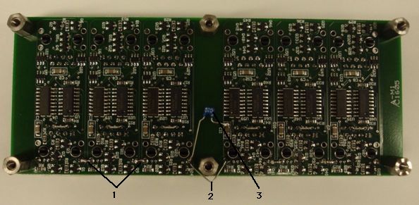
The A2059B solves this problem by connecting all the connector shields together, connecting them to the chassis, and connecting them to the local, shared (see above) 0-V with a 100-nF capacitor.
Approximately one in ten A2059A channels fail at the end of a long root cable. The failure manifests itself most clearly as erratic images from a BCAM, and occurs when the driver disables the T+ and T− lines to turn on a light source attached to another driver socket. With a 40-m root cable, one in four images is white, as if saturated. On the end of an 80-m root cable, as shown here, every other image is white. When the T+ and T− lines are disabled, a 10 kΩ resistor on the driver pulls T+ towards +5 V, and T− with it through the 100-Ω terminating resistor on the A2059A. On the end of a long cable, this pull-up can take several miliseconds. Diodes in the repeater clamp the LVDS lines to around 3.9 V. In a faulty repeater channel, the SN65LVDS180D receiver chip (U1 in the schematic) registers logic transitions on T+/T− as they pass through the neighborhood of 2.7 V. When we replace U1 with another chip of the same type, some of the replacement chips will act the same way, while others will not. If, on the other hand, we replace U1 with an SN65LVDM180D, the problem is fixed. It's not clear that the LVDS chip is violating its data sheet, but we never observe this problem on multiplexers, which use the same chip and would show the same symptom. We conclude that 10% of new chips behave this way.

The A2059B solves this problem by adding a 10-kΩ pull-down resistor to the T− line on the patch panel.
Note: All our schematics and Gerber files are distributed under the GNU General Public License.
Here are the two pages of the A2058 circuit diagram, which is repeated six times on the A2059:
Page 1: LVDS TransceiverPrinted circuit board files: A205901A