| Schematic | PCB |
The TC237 Minimal Head (A2070) holds a TC237 gray-scale image sensor or a TC236P color image sensor. These sensors provide 500 rows and 660 columns of active image pixels that are each 7.4-μm square for a total image area of 5.9 mm × 3.7 mm. The A2070 provides an 8-way 1-mm flex socket for connection to a control circuit such as the Dual Rasnik Head (A2072). We can connect the A2070 to circuits designed for the TC255P also, such as the Azimuthal BCAM Head (A2048), Proximity Camera Head (A2047), Polar BCAM Head (A2051). The LWDAQ Driver, however, must support the TC237 device type.

The TC237 is a frame store sensor. It consists of an image area and a storage area. The image area is exposed to light. The storage area is in darkness. We acquire an image in the image area, move it into the storage area row by row, and read it out from the storage area pixel by pixel.
The TC237 is a gray-scale image sensor, while the TC236P is a color image sensor. Both are device type TC237 (5) in the LWDAQ software and firmware. When read out by the LWDAQ hardware, they produce images with 500 rows and 690 columns. The left-most thirty columns are black reference columns.
The TC236P uses red, blue, and green color filters to measure the relative intensities of the three primary colors in incident light. We obtain fine color images with the TC236P, but the part is now obsolete, along with the TC255P. Texas Instruments manufactured all these CCDs, and all of them operate in almost exactly the same way. The only remaining active part in the series is the TC236B. The A2070 allows us to convert our existing cameras from the TC255P to the TC237 with the minimum of re-work.
The pinout of the A2070's flex connector is compatible with that of the TC255P Minimal Head (A2016). We can connect the A2070 to any LWDAQ Device that is compatible with the A2016. The amplitude of the output signal from the TC237 is one third that of the TC255P. Thus any LWDAQ Device designed for use with the TC255P will provide a dim image when used with the A2070. The A2047C, A2048C, A2051C are all examples of TC255P circuits modified to provide a brighter image from TC237 and TC236P sensors. Most TC255P Devices permit this modification, but the Inplane Sensor Head (A2036) does not.
The following table lists the avialable and planned versions of the A2070. We describe each version by giving the location of the flex connector, J1, with respect to the image sensor. To define our directions: up, down, left, right, top, bottom, we look straight down at the image sensor, with Pin 1 of the package on the top-left. The top side of the PCB (printed circuit board) is the side upon which the image sensor is mounted. The bottom side is the other side of the PCB. The directions up, down, left, and right lie in the plane of the PCB. When we say the connector is oriented vertically, we mean the length of the connector is in the up-down direction. Horizontal (H) orientation puts the length of the connector in the left-right direction. Pin 1 of the flex connector might be marked on the top of bottom silk screen with a small 1 numeral, or it might not be so marked. But Pin 1 will always be distinguished from the other eight pins of the flex connector footprint by its square pad shape. Similarly, Pin 1 of the image sensor socket is square. The CCD can either sit 1.2 mm off the circuit board, or flush with the circuit board. We specify "raised" or "flush" in the table.
| Version | J1 Location and Orientation | Intended Master Device |
|---|---|---|
| A2070A | top-side, horizontal, pin-1 left, below sensor, mounting holes, raised | A2051C |
| A2070B | bottom-side, vertical, pin-1 down, left of sensor, raised | A2072A |
| A2070C | bottom-side, vertical, pin-1 down, left of sensor, raised | A2072A |
| A2070D | top-side, vertical, pin-1 up, left of sensor, CMT821 lens mount, mounting holes, raised | A2072A |
| A2070E | top-side, vertical, pin-1 up, left of sensor, CMT821 lens mount, mounting holes, flush | A2072A |
To capture images from any version of the TC237 Minimal Head (A2070), connect it to any device that supports the TC255P Minimal Head (A2016) and whose output gain has been increased to suit the TC237, or connect it to any device designed specifically for the A2070, such as the Dual Rasnik Head (A2072). Open the Camera Instrument and press the TC237 button on the instrument panel (these buttons are available in LWDAQ 7.7 or later). Pressing the TC237 button will configure the camera for the TC237.
| Parameter | Value | Description |
|---|---|---|
| daq_device_type | 5 | Specifies TC237 device for LWDAQ firmware |
| daq_image_height | 500 | Number of rows |
| daq_image_width | 690 | Number of columns |
| daq_image_left | 35 | Left edge of active area |
| daq_image_top | 5 | Top edge of active area |
| daq_image_right | 685 | Right edge of active area |
| daq_image_bottom | 495 | Bottom edge of active area |
In addition to the above, be sure to set daq_device_element correctly for our LWDAQ device. The single-ended TC237 polar BCAM, for example, uses a Black Polar BCAM Head (A2051L) connected to an A2070A to provide a forward-looking camera. You must set daq_device_element to 2 to select the forward camera, or else the A2051L will try to use its non-existent rear-facing camera.
You can configure the Camera Instrument in earlier versions of LWDAQ using the following script. Cut and past the script from this page into the Toolmaker window and execute.
set LWDAQ_info_Camera(daq_image_left) "35"
set LWDAQ_info_Camera(daq_image_bottom) "495"
set LWDAQ_info_Camera(daq_image_top) "5"
set LWDAQ_info_Camera(daq_image_right) "685"
set LWDAQ_info_Camera(daq_image_width) "690"
set LWDAQ_info_Camera(daq_image_height) "500"
set LWDAQ_info_Camera(daq_device_type) "5"
set LWDAQ_info_Camera(daq_device_element) "2"
Here is an example image taken with the TC237 and a DSL821 lens held in a CMT821 lens holder.
The same lens holder will accept the DSL216 fish-eye lens. We point this lens at the wall of our lab and obatin the 185° hemispherical view shown here. The lens 3.6-mm image circle just fits within the TC237 image area. The DSL215 has a 4.7-mm image circle, as you can see here.
You can configure the BCAM and Rasnik instruments for the TC237 by pressing the TC237 button in the instrument's information panel. Or you can configure the BCAM by running the following script in the Toomaker (just cut and paste from this page into the Toolmaker window).
set LWDAQ_info_BCAM(daq_image_left) "35"
set LWDAQ_info_BCAM(daq_image_bottom) "495"
set LWDAQ_info_BCAM(daq_image_top) "5"
set LWDAQ_info_BCAM(daq_image_right) "685"
set LWDAQ_info_BCAM(daq_image_width) "690"
set LWDAQ_info_BCAM(daq_image_height) "500"
set LWDAQ_info_BCAM(daq_device_type) "5"
set LWDAQ_info_BCAM(daq_device_element) "2"
set LWDAQ_info_BCAM(analysis_pixel_size_um) "7.4"
In the LWDAQ hardware logic, the TC237 has device type 4. Only LWDAQ Drivers programmed after 21-DEC-09 are able to read out TC237 devices. If you are using a LWDAQ Driver with Ethernet Interface (A2037E), you need firmware version 14 or higher. The LWDAQ Driver with VME Interface (A2037A) does not support the TC237.
The color version of the TC237 is the TC236P. The color CCD has been obsolete for ten years, but it so happens that we have two in our lab. To obtain an image from one of them, we set our camera up just as we do for the TC237, but we use a different form of intensification. Instead of exact we use exact_rggb. The "rggb" tells the LWDAQ software to divide the image into four-pixel squares in which the top-left pixel is red, and the bottom-left is blue, with the other two being green. The TC236P is approximately half as sensitive to light as the TC237, a consequence of its color filters.
The TC237 pixels are each 7.4 μm square. We define the origin of the sensor area to be its bottom-left corner, as shown below. This sensor area is read out by the LWDAQ and displayed upon the screen with the origin in the top-left corner of the top-left pixel. In the sensor, x is left to right and y is bottom to top. In the image, x is also left to right, but now y is top to bottom.

The active image area on the sensor is 4.884 mm × 3.700 mm, consisting of 660 active columns and 500 active rows. The image on our computer screen, however, contains 690 active columns and 500 active rows. The first 30 columns on the left side of the image are black-level columns. Thus the final image corresponds to an area 5.106 mm × 3.700 mm.
The figure below is a drawing of the TC237 package, as taken from its data sheet.
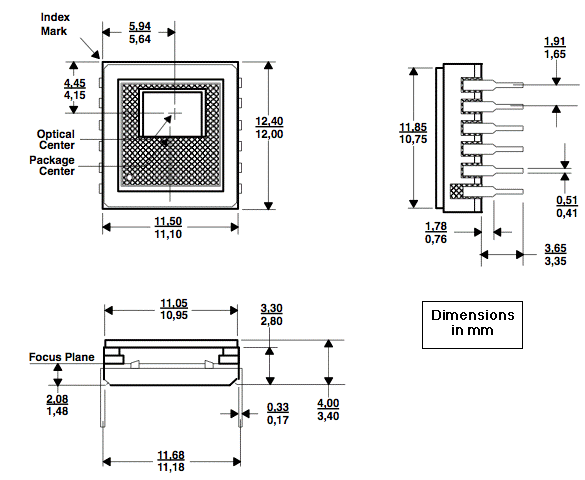
The twelve-lead frame package is unusual. We have found no socket that will accept the package. We solder the TC237 directly into its circuit board. It is important that the holes of the package are only just large enough for the tips of the leads, or else it is possible to push the package farther into the board by force, so that the thicker shoulders of the pins enter the holes. We use 25-mil holes (0.63 mm diameter).
The flex connector on the A2070 brings in +12 V, 0 V, and three clock signals (IAG, SRG, SAG). It carries away the sensor output (OUT). The clock signals switch between +2 V and −11V. The sensor output is an analog voltage. It's black-level is 10V, and white-level is roughly 9.7V. The connector provided by the A2070 is an eight-way 1-mm pitch flex connector for use with an 8-way 1-mm pitch flex cable. We use an eight-way connector for backward-compatibility with the A2016, which required a forth clock signal (ABG) to implement its anti-blooming function. The A2070 implements anti-blooming with a fixed voltage generated by a resitive dividor.
Inside an aluminum enclosure, we notice no degradation of image quality for flex cables up to 15 cm. We are able to acquire images with 45-cm flex cables, but they have diagonal lines of electronic noise. We chose the pin-out of the eight-way flex connector so that plugging the flex cable in the wrong way around would cause no damage to either the TC255P or the control electronics.
The TC237 data sheet specifies clock and bias voltages with the assumption that we connect the substrate of the chip to 10 V. If we instead connect the substrate to 0 V, and so apply negative voltages to the clock inputs, we see that the TC237 and indeed the TC236P also, accept the same voltage levels as the TC255P. The only input that differs from the TC255P is the anti-blooming control pin, which is named ODB, and is U1-1 in our schematic. The following table gives the TC237 voltage levels with respect to a substrate at 0 V.
| Pin | Name | Voltage (V) | Function |
|---|---|---|---|
| 1 | ODB | 5 | Anti-Blooming Disabled |
| 1 | ODB | 6 | Anti-Blooming Enabled |
| 1 | ODB | 16 | Clear All Charge from CCD |
| 2, 12 | IAG | 2 | Image Area Gate HI (Row in Transition) |
| 2, 12 | IAG | −10 | Image Area Gate LO (Row in Place) |
| 3, 9 | SUB | 0 | Substrate |
| 4 | ADB | 12 | Amplifier Drain Biase |
| 5 | OUT1 | 9-10 | Secondary Pixel Output |
| 6 | OUT2 | 9-10 | Primary Pixel Output |
| 7 | RST | 2 | Reset HI (Asserted) |
| 7 | RST | −10 | Reset LO (Unasserted) |
| 8 | SRG | 2 | Serial Register Gate HI (No Output) |
| 8 | SRG | −10 | Serial Register Gate LO (Pixel Output) |
| 9, 10 | SAG | 2 | Storage Area Gate HI (Row in Transition) |
| 9, 10 | SAG | 2 | Storage Area Gate LO (Row in Place) |
Although the TC237 data sheet recommends that we apply RST just before and just after the rising edge of SRG, the charge-to-voltage converter used at the output of the TC237 is almost identical to the one used in the TC255P, where RST is connected internally to SRG. We experimented with SRG and RST and found that we could connect RST directly to SRG and suffer no loss of image quality. Thus RST and SRG are connected on the A2070.
The anti-blooming control provided by the TC237 is not compatible with the TC255P. The TC255P required clocking of the anti-blooming gate during exposure, or a constant bias voltage of −2.5 V. We applied the anti-blooming clock or bias to the ABG pin. The TC237 requires only a bias voltage, but this voltage dictates the anti-blooming behavior. We apply the anti-blooming bias to the ODB pin. The higher the value of ODB, the more anti-blooming and the smaller the pixel capacity. In our alignment sensor applications, we like large well capacity with linear response. But if we apply too low a voltage on ODB, the dark current starts to rise dramatically, which reduces our neutron radiation tolerance. With ODB at at 4 V we observed saturation contrast of 310 mV at OUT2, and no immunity to blooming. Any pixel that overlows spills its charge into the pixels above and below. With ODB at 5 V we see some suppression of blooming, but no reduction in saturation contrast. With ODB at 6 V we see better suppression of blooming, but saturation contrast drops to 270 mV. With ODB at 7 V we see complete suppression of blooming but contrast drops to only 160 mV. After some experimentation, we settle upon using a 10-kΩ resistor in series with a 5.6-V zener diode to set the voltage at around 5.4 V. We find this gives us image contrast of around 300 mV and good anti-blooming.
The TC237 and TC236P are both members of a family of CCDs designed by a collaboration between the Jet Propulsion Laboratory and Texas Instruments. The CCDs are designed to be resistant to ionizing radiation. The TC255P is also a member of this family. We tested the TC255P in neutron radiation twice. We report on our 1998 test in here and our 1999 test here. We summarize the results of ionizing and neutron radiation tests in Pre-Production Radiation Tests. Our ionizing tests indicate that the TC255P can tolerate over 1 Mrad when used with the LWDAQ. Neutron radiation increases the TC255P dark current. After 1012 1-MeV eq. n/cm2, the dark current at room temperature will fill up the pixels in only 400 ms, as compared to roughly 4 s for an un-damaged CCD. By keeping our exposure times below 40 ms, we can tolerate such a dark current, and so the TC255Ps in the ATLAS detector can tolerate 1012 1-MeV eq. n/cm2, which is over ten times the maximum dose we expect at full luminosity for ten years. We suspect that the ionizing and neutron radiation tolerance of the TC237 is similar to that of the TC255P.
Note: All our schematics and Gerber files are distributed for free under the GNU General Public License.
The flex connector, J1, is a 1-mm flex cable socket. We buy ours from Digikey. Some sockets have contacts on one side, others have contacts on both sides. The table below gives the TC237 connections present on the pins of the eight-way socket. We chose the pin-out on the socket so that plugging the flex cable in the wrong way will not damage the image sensor or the control electronics.
| Signal | J1 Pin | U1 Pin | Full Name |
| OUT | 3 | 4 | output |
| SAG | 4 | 6 | storage area gate |
| SRG | 8 | 5 | serial register gate |
| +12V | 1 | 2 | drain voltage supply |
| 0V | 5 | 3 | substrate voltage supply |
| IAG | 6 | 1,7 | image area gates |
The sensor, U1, must be soldered directly onto the printed circuit board. We know of no sockets for the 12-lead frame package, nor can we find SIP sockets with the correct lead spacing.
The images we obtain with the A2070 have a black level intensity of around 150 counts (we measure intensity in eight-bit ADC counts, so they are 0 to 255) and saturation intensity of around 250 counts. Thus the black level takes up most of the dynamic range of our ADC. The high black level is the result of our tying the TC237's reset gate (RST) to its serial register gate (SRG). When our LWDAQ driver clamps to the black level, it is clamping to the output with the reset gate asserted. When we release RST and at the same time clock a new pixel onto the output with SRG, for they are tied together, what appears at the output is not only the pixel intensity but also the reset charge.
A better way to operate the sensor is to raise RST and SRG to +2 V for 125 ns, then allow RST to fall to −11 V while keepingn SRG at +2 V. Now we clamp to the black level, because the reset charge is already on the output transistor. After we clamp, we let SRG drop to −11 V and the pixel appears at the output. We tied SRG and RST together so that we could use the TC237 with our existing TC255 devices, such as those listed in above. Despite the 150-count black level, the images we obtain are still sharp and clear.
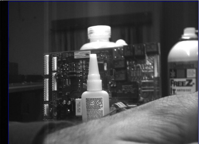
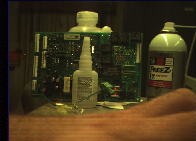
The A207201B printed circuit board is missing the connection between J1-5 and U1-3, so we must make this connection with a wire link. Another error on this same board is the silkscreen identification, which says A207001A.