Any silicon image sensor can be used as an ionizing radiation dosimeter. The sensor detects light by converting individual photons into individual electrons. These electrons are accumulated in the sensor pixels. The brightness of each pixel is proportional to the charge it accumulates. The sensor detects ionizing radiation in the same way, except each ionizing photon or charged particle is converted into a large number of electrons. It takes 1.1 eV to promote an electron into silicon's conduction band. If an x-ray deposits 11 keV in a pixel, ten thousand electrons will remain in the pixel as evidence of the interaction. The brightness of each pixel is proportional to the energy deposited by the ionizing radiation in each pixel. At low dose rates, we see occasional spots of light in the image. Each spot correspond to a single ionizing interaction. At high dose rates, we see a flat gray or white image where the charge from individual interactions has blurred together.
If we knew the charge-accumulating volume of an image sensor, we could combine this with the density of silicon to obtain a direct measurement of the ionizing dose in units of J/kg in silicon, or Gray in Si. Because we are interested in damage done by radiation to silicon circuits, the unit of Gray in silicon is precisely the one we wish to obtain. Thus the silicon image sensor is well-suited to a study of radiation damage in electronics. The width and height of a sensor's pixels are specified by its data sheet. But the effective depth of the pixels as they extend into the silicon is not specified. Indeed, the effective depth might be a function of the radiation energy, which would undermine the proportionality we desire between charge and deposited energy.
In addition to measuring ionizing dose rate, it turns out that silicon image sensors can make a crude measurement of accumulated neutron dose as well. Fast neutrons have a chance of colliding with one of the silicon nuclei, which damages the silicone lattice. This damage increases the sensor dark current, which gives rise to a gradient of intensity from the top to the bottom of the image.
The TC255P, TC237, KAF0400, and ICX424 are all CCD image sensors we can use with the LWDAQ. The Dosimeter Instrument obtains images from such sensors and analyzes them so as to provide measurements of ionizing dose rate and accumulated neutron dose. In this report we summarize the performance of dosimeters made with the image sensors available to the LWDAQ. You will find our experimental results in a spreadsheet here (Open Office). For a description of our radiation sources and dosimeters, see Irradiation Apparatus.
The TC255P provides a charge-collecting area 3.4 mm × 2.4 mm with 10 μm square pixels. The ICX424 provides a 5.18 mm × 3.85 mm image area with 7.4-μm pixels. The ICX424 provides a 5.18 mm × 3.85 mm image area with 7.4-μm pixels. All three sensors are designed to detect visible light images in their array of pixels.
| Property | TC255P | ICX424 | KAF0400 |
|---|---|---|---|
| Sensor Width (mm) | 3.44 | 5.18 | 7.20 |
| Sensor Height (mm) | 2.44 | 3.85 | 4.68 |
| Pixel Width (μm) | 10 | 7.4 | 9.0 |
| Pixel Height (μm) | 10 | 7.4 | 9.0 |
| Rows (number) | 244 | 520 | 520 |
| Columns (number) | 344 | 700 | 800 |
| Pixel Capacity (k-electrons) | 60 | 50 | 100 |
| Readout Sensitivity (counts/electron) | 1/300 | 1/250 | 1/500 |
| Readout Speed (Mpixels/second) | 2.0 | 2.0 | 2.0 |
| Readout Speed (μs/row) | 172 | 350 | 400 |
| Example Circuit | A2016 | A2075 | A2061 |
It takes 1.1 eV to promote an electron from silicon's valence band to its conduction band. This is true of all silicon image sensors. Provided the photon energy is above 1.1 eV, the sensor has a chance of detecting the illumination. Some photons, however, will be absorbed in features on top of the pixel, or reflected from its surface. The following plots show relative sensitivity versus wavelength for three image sensors. The sensitivity drops to zero at 1050 nm because this is the wavelength at which the photon energy drops below 1.1 eV.


The quantum efficiency is proportion of photons that are converted into electrons. The relative response is a measure of the number of electrons generated per unit energy of illumination incident upon the detector, with some wavelength picked as a reference for normalization. The ICX424 produces 60% as many electrons per Joule at 400 nm as at 500 nm. Some of this drop in response is due to the reflection of blue light from the sensor surface and some is due to the fact that each photon carries more energy. Energy above 1.1 eV is wasted.
The poor sensitivity of the TC255P to blue light suggests that it is a front-illuminated device with features on top of the pixel that absorb blue light. The ICX424 and KAF0400 sensitivity to blue light suggests they are back-illuminated device, with a bare silicon surface to receive light.
The TC255P provides a second array of pixels adjacent to the first, into which we shift the image lies before we read out the pixel intensities. This storage area is masked from light by aluminum. The ICX424 provides a second array also, but its second array pixels are beneath the image array pixels, deeper in the silicon crystal upon which the image sensor is build. The transfer of all pixels into the second array is simultaneous and immediate. The KAF0400 does not provide a secondary pixel array. We read the pixels directly from the image area.
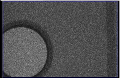
Our hope is to use the image sensors in existing optical cameras as radiation dosimeters. In that case, we would like our detection of ionizing radiation to be undisturbed by ambient light. We use the secondary arrays of pixels provided by the TC255P and ICX424 sensors because these are masked from light by aluminum and silicon respectively. But it turns out that the secondary pixels in the TC255P, those in the storage area, are not square. The image below shows a contact print of a sphere taken with the TC255P storage area.
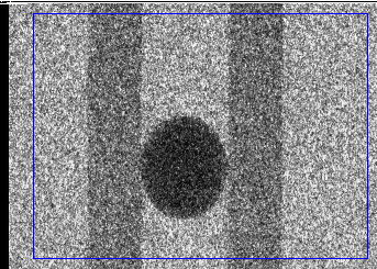
In the image above, the sphere width is 79 pixels, which means the pixel width in the storage area is 10 μm as it is in the image area. The sphere height is 93 pixels, so the pixel height is only 8.5 μm.
The KAF0400 has no secondary array, which means must eliminate ambient light when we use it to detect radiation or take x-ray images. We can place black tape over the sensor glass. This sensor takes over a minute to fill up with dark current at room temperature, so it is suitable for long x-ray exposures through thick metallic objects for the purpose of internal inspection.
In addition to the bare KAF0400 and its pin-compatible successor the KAF0401E, we have KAF0400s with phosphor coatings 30-120 μm deep. These coatings increase the effective depth of the image pixels by a factor of ten or more, but light from the top layer of phosphor spreads out in all direction. Thus a radiation hit in the top of the phospher will be spread out by something like the depth of the phosphor. We show a KAF0400 phosphor contact print below.
An image sensor measures the charge deposited in each pixel. We can convert this charge into deposited energy by multiplying by 1.1 eV. But if we want to calculate the energy deposited per kilogram of silicon, we need to know the volume of each pixel. We know the width and height of our image pixels, but we do do not know their effective depth. The depth is not specified in the sensor data sheets. Furthermore, we prefer to use the sensor's secondary, light-shielded pixels for radiation detection, if such exist. Thus it is the depth of these secondary pixels that concerns us, not the light-sensitive pixels.
Each pixel consists of a potential well that collects the electrons liberated by ionizing energy within the pixel. Thus the depth of the pixel is the same as the depth of this potential well. The depth of the potential well is dictated by the silicon doping and the voltages we apply to the pixel clock phases. Thus we see no reason to expect the depth of the pixel change with the nature of the applied radiation. It may be that ionizing radiation is absorbed before it can reach the pixels, as it can be by the sensor glass, But the effective pixel depth should remain the same for all incident ionizing radiation.
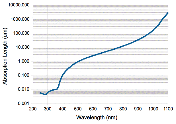
One way to estimate the pixel depth is to deduce it from the sensor's quantum efficiency. The graph below shows the measured absorption coefficient of light in silicon. Suppose we assume that the secondary pixels in the TC255P are identical to image pixels, except for a covering of aluminum. The quantum efficiency of the TC255P image sensor at 800 nm is 50%. The absorption depth of 800-nm light in silicon is 10 μm. This suggests that the effective depth of the TC255P image pixels is at least 7 μm. The quantum efficienty at 600 nm is 30%. This suggests a pixel dept of at least 1 μm. The pixels could be much deeper, with reflection accounting for loss, or they could be shallower and absorption could be greater because of light-absorbing coatings on the sensor surface.
Another way to estimate pixel depth is to use a known ionizing radiation dose and measure the charge accumulated in the pixels. This amounts to a direct calibration of the dosimeter from which we can deduce an effective pixel depth. The authors Awaki et al. used high-energy particles to measure the effective thickness of pixels in a front-illuminated CCD, and obtained a value of 6.7 μm. Studies with back-illuminated image sensors suggest effective depths up to 70 μm.
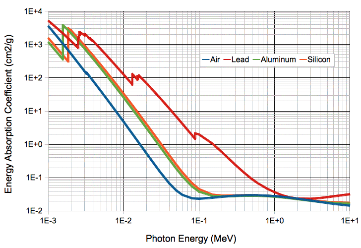
We have calibrated ionizing dosimeters and various radiation sources. The measured absorption coefficient of photons in silicon might allow us to estimate the effective pixel depth of our radiation-detecting pixels. The following graph translates the absorption coefficient in cm2/g into absorption length in mm. One graph shows the depth of Si that will interact with 63% of photons. The other shows the depth of Si that will absorb 63% of the photon energy.

Any interaction between a photon and the silicon of our dosimeter pixels will result in charge deposition and detection. If we know the energy and fluence of a photon source passing perpendicularly through our dosimeter pixels, we might be able to use the measured dosimeter hit rate to estimate the effective thickness of its pixels. As we show below, however, this calibrtion is compromised by interactions with the sensor glass, which produce hits that do not correspond to absorption in the pixel silicon.
Instead of using hit counts, we can measure the energy deposited in our pixels for a known radiation dose. When we measure the dose produced by one of our radiation sources, we use a calibrated ionizing chamber, as we describe elsewhere. This ionizing chamber allows us to measure the dose in units of Roentgen. One Roentgen = 1 R = 2.58×10⁻⁴ Colombs of charge deposited per kilogram of air. We convert into Joules per Kilogram in using the ionization energy of air, which is 34 J/kg. Thus 1 R = 0.00877 J/kg = 1 Gray in Air = 1 Gy in Air. To convert from J/kg in air to J/kg in silicon, we use the spectrum of our ionizing radiation and the relative absorption coefficients of this radiation in silicon and air.
For x-rays between 5 keV and 50 keV, the absorption coefficient of silicon is roughly 7.3 times greater than for air. The same radiation flux will deposit 7.3 times more energy in silicon than in air. When we irradiate an image sensor with x-rays in this range, we take Gray in Air and multiply by 7.3 to obtain Gray in Si. For x-rays between 5 keV and 50 keV we have 1 R = 0.064 Gy in Si. With this value of energy per kilogram, and using the area of the sensor, the total charge accumulated, and the density of silicon, we can obtain an estimate of the effective pixel depth.
In X-Ray Detection, we measure the sensitivity of the TC255P storage area pixels to x-rays of energy 10-60 keV. We find it to be 614 counts/pixel/R. If we assume each count represents 300 electrons, each electron 1.1 eV, we obtain a energy density of 3.24×10⁻¹⁴ J/px/R. If we assume ionization energy 34 eV for air then 1 R represents 8.77×10⁻³ J/kg of air. This same dose should deposit roughly 7.3 times more energy in Si than Air, or 64.0×10⁻³ J/kg. The mass of one pixel should be 5.35×10⁻¹³ kg. The density of Si is 2.65×10³ kg/m3, so the volume of one pixel is 2.01×10⁻¹⁶ m3. The TC255P storage are pixels are 10 μm wide and 8.5 μm high, so they must be roughly 2.4 μm thick. When we use the TC255P image area, the pixels are 10 μm square and the sensitivity is 975 counts/pixel/R, which suggests a depth of roughly 3.2 μm.
We repeated our x-ray measurements with the TC255P image area pixels in a dark room, with tape over the image sensor. The image area pixels are 10 μm square and might be deeper than the storage area pixels. We obtained a sensitivity only slightly greater than for the storage area pixels, leading to an estimate of pixel depth of 2.2 μm.
We have four estimates of TC255P pixel depth. From 800-nm light in the TC255P we estimate >7 μm in the image pixels. From 600-nm light we estimate >2 μm. From x-rays we estimate 2.4 μm in the storage area and 2.2 μm in the image area. Thus our optical measurements disagree with our x-ray measurements.
The average energy of our x-ray spectrum is around 30 keV. The continuous slowing-down approximation for electrons in silicon, which we plot here, implies that a 20-keV electron will travel around 5 μm through silicon. If the average interaction takes place 3.5 μm into a pixel 7 μm deep, and generated a 20-keV electron that traveled 5 μm, we would might lose 50% of deposited energy, thus causing our effective pixel depth to be reduced by a factor of two. This is the best explanation we can come up with for the disagreement between our optical and x-ray estimates of the pixel depth.
Fast neutrons knock silicon atoms out of place within the silicon crystal that forms the pixels of our image sensor. Damage sites in the silicon are places where electron-hole pairs can be created more easily by thermal agitation. Any accumulation of charge in a pixel that is generated within the pixel itself we call dark current. As damage in the silicon accumulates, the image sensor's dark current increases. By measuring the dark current, we can measure the amount of damage and therefore the total accumulated neutron dose. The dark current is, however, a strong function of temperature, so we must know the temperature to within a fraction of a degree if we are to make a good measurement of the neutron dose. In the ATLAS detector's end-cap alignment system, we happen to know the temperature of all aluminum parts to within 0.1°C.
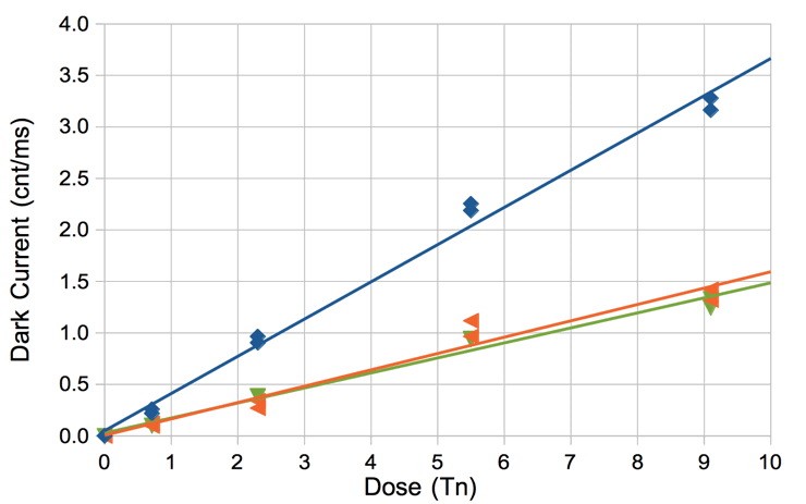
We subjected several TC255P image sensor to fast neutrons and observed an increase in their dark current. We present our measurements and conclusions in two papers Irradiation of the TC255P CCD by Fast Neutrons, Part One and Irradiation of the TC255P CCD by Fast Neutrons, Part Two. The dark current increases linearly with accumulated fast neutron dose, and exponentially with temperature. For each 1012 1-MeV eq.n/cm2 = 1 Tn of fast neutron dose, the dark current at 20°C increased by 0.28 cnt/ms/Tn in Part One, and 0.26 cnt/ms/Tn in Part Two. Here, our units for dark current are 8-bit ADC counts, because our LWDAQ data acquisition system reads out images with eight-bit precision. For each 8.5°C increase in temperature, the dark current doubles.
In Alignment for High Luminosity we show how image sensor dark current can be used as a measure of accumulated neutron dose. The dark current is proportional to the gradient of the image intensity in the vertical direction. The rows at the bottom of the image are read out last, and so spend more time gathering dark current than those at the top. In the case of the LWDAQ Driver (A2037) and Inplane Sensor Head (A2036) the readout time is 197 μs per row. Thus each successive row has spend 197 μs longer in the sensor, and has accumulated dark current for an additional 197 μs. The top rows spend 244 × 197 μs = 48 ms longer in the sensor than the bottom rows. Images from sensors damaged by fast neutrons are brighter at the bottom than at the top.
As shown below, the damage caused by neutrons diminishes over time, through annealing at room temperature. When we normalize the damage rates to 20°C we get 0.26 cnt/ms/Tn one month after irradiation, and 0.14 cnt/ms/Tn twenty years after irradiation.
The slope of intensity from has units cnt/row. The first number in the Dosimeter Instrument result is the intensity slope in cnt/row, calculated within the analysis bounds. The dosimeter's measurement of vertical slope has resolution 0.0001 cnt/row = 0.0005 cnt/ms. A non-existent sensor gives us an average slope of 0.0000 cnt/ms. A new TC255P gives us an average slope of 0.001 cnt/ms. Given a damage rate of 0.28 cnt/ms/Tn, a resolution of 0.001 cnt/ms provides a neutron dose resolution of 0.038 Tn.
In addition to a distributed dark current, fast neutrons also create bright pixels that stand out from the background. These pixels are rare, but their are easy to find, because they are bright from the first moment they appear. By isolating these pixels and adding their intensities together, we obtain a measuremnt of neutron dose that is far more sensitive than that of the intensity slope. Any pixel above a threshold intensity is a bright pixel, and the intensity of this pixel we take to be its intensity above a background intensity. The Dosimeter Instrument permits us to specify background and threshold in many ways. The threshold string "5 $" specifies a background equal to the average intensit of the image, and a threshold five counts above the average. The second number in the Dosimeter output string is the bright pixel charge density, which is the combined bright pixel intensity divided by the number of pixels in the analysis boundaries. We take a 100-ms exposure in the dark so as to obtain the greatest charge density, and divide by 100 to obtain the bright-pixel dark current in cnt/ms/px. The bright pixel dark current is proportional to neutron. In the ATLAS experiment, we find that the bright-pixel dark current is roughly twenty times smaller than the intensity-slope dark current, but our precision in measuring bright-pixel dark current is sufficient to detect doses of 0.0001 Tn.
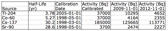
For low dose rates, we can see individual ionizing interactions in our dosimeter image. We call these hits. We presented our first observations of radiation hits in a talk at CERN in November 2009 (Radiation Detection with Alignment Sensors). We have a set of four low-activity laboratory radiation sources, shown here. The following table gives the activity of these sources at various dates.
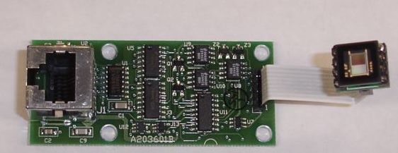
We used these to generate hits in a TC255P image sensor. To read out the sensor we used a TC255P Minimal Head (A2016) and Inplane Sensor Head (A2036). These are two of each such circuits in every muon chamber of the ATLAS end-cap alignment system.
We began with the Co-60 source and a TC255P image sensor. We cover the image sensor with tape and put the source on top of the tape. The sensor occupies an area 2.4 mm × 3.4 mm at range 4 mm from the source, so roughly 3% of the decay products set off in the direction of the image sensor. To the first approximation, each Co-60 decay produces two gamma rays, one of energy 1.2 MeV and another of energy 1.3 MeV. Between the source in its nylon package and the silicon of our dosimeter pixels, we have the following material: a few microns of Al, 2 mm of nylon, 0.2 mm of tape, 0.8 mm of glass, and 1 mm of air. These materials will stop only a tiny fraction of 1-MeV gamma rays. Almost all the gamma rays heading towards the image sensor pass through it. The activity of the source at the time of our experiments was 4.2 kBq, which means we will get 8400 gamma rays per second. Of these, 250 will pass through our dosimeter sensor per second, and 25 in a single 100-ms exposure.
The absorption depth of 1.2-MeV gammas in silicon is roughly 70 m. The effective depth of our dosimeter pixels is roughly 10 μm. We expect only 140 out of every million of Co-60 gamma rays to be absorbed directly in the pixels, which would mean an average of only 0.0036 interactions per 100 ms exposure.
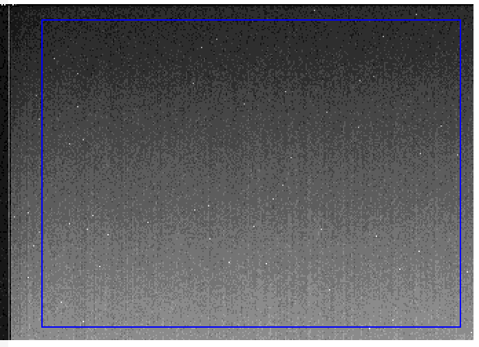
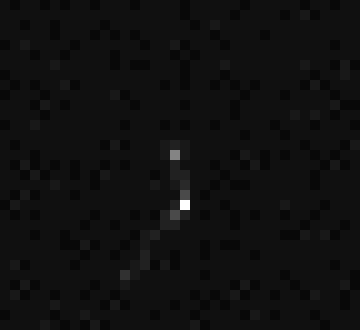
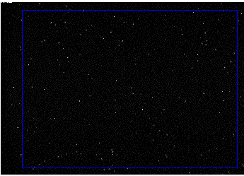
We captured 100-ms images with the Dosimeter Instrument and set the hit intensity threshold to two counts above the average intensity in the image (threshold code "2 $"). Over the course of 1413 images, 6.4% of images contained one or more hits. Some images contained two or three hits, as shown below.
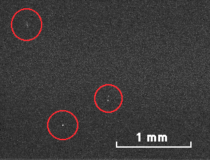
The Dosimeter calculates for us the total intensity above threshold of each spot. It subtracts the threshold from each pixel in the hit, sets the result to zero if negative, and adds to the sum for the hit. The central hit in the above image has brightness 40 counts. In our eight-bit readout, one eight-bit count represents 300 electrons (saturation is at 200 counts and pixel capacity is 60,000 electrons). The band gap voltage for silicon is 1.1 V. One count corresponds to roughly 330 eV of ionizing energy. The central hit represents the deposition of roughly 13 keV of ionizing energy.
It is impossibly unlikely that three gammas would interact with the sensor pixels in the same 100-ms exposure. Furthermore, the 6.4% hit rate is far higher than our expected 0.36% hit rate for direct interactions between a gamma ray and the pixel silicon. We conclude that the vast majority of the hits we see are the result of interactions between the Co-60 gammas and the image sensor's glass window. Such interactions will create a shower of electrons, and any electron with more than a few keV of energy passing through our dosimeter sensor will be detected as a hit. The glass, being 0.8 mm thick with absorption coeffient similar to silicon, will interact with roughly 1.1% of 1.2-MeV gamma rays. Of the 250 gamma rays passing through the glass and the sensor every second, we expect 1.1% of them to interact with the glass, which gives us an average of 0.28 interactions per 100-ms exposure. These 0.28 interactions will produce electrons by Compton scattering. Our hit rate of 6.4% suggests that only 22% of such interactions produce an electron that moves in the direction of the sensor and is energetic enough to reach the pixels.
Most of the hits we see with the Co-60 source have energy a few keV. But roughly 0.2% of every thousand images contains a bright and concentrated hit like the one shown below. The energy is concentrated in a single pixel, which contains roughly thirty thousand electrons, indicating 35 keV of ionizing energy. We suspect the pixel lay at the end of the path of an electron knocked out by Compton scattering of a gamma ray very close to or within the pixel. Indeed, a concentrated hit rate of 0.2% is consistent with 1.2-MeV gammas scattering in a 20-μm thickness of silicon.

The following figure shows a smeared hit from a Co-60 radiation source. The total hit energy is approximately 20 keV summed over the bright pixels. Only one in a hundred hits is smeared. We suspect the smeared hits are caused by Compton scattering in which the electron emerges at ninety degrees to the scattered photon.
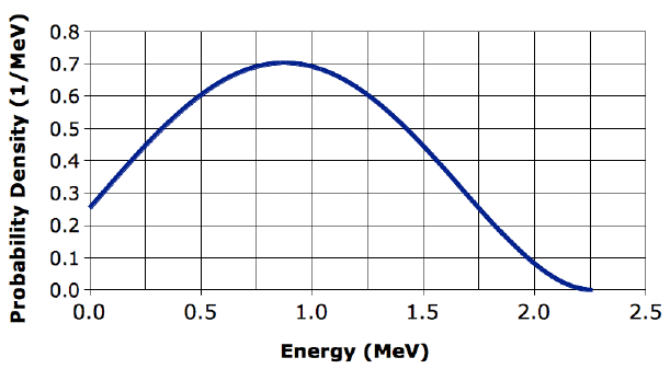
We now work with our Sr-90 source. Its activity at the time of our first experiments was 2.5 kBq. Each Sr-90 decay produces two electrons (beta particles) with maximum energies 0.55 and 2.3 MeV. Their energies are distributed according to a Fermi-Dirac distribution. We present this distribution for the 2.3-MeV electron below. The average energy of this electron is 0.92 MeV.
We place the Sr-90 source in front of our sensor. As before, we have between the source and sensor: a few microns of Al, 2 mm of nylon, 0.2 mm of tape, 0.8 mm of glass, and 1 mm of air. We expect 3% of the emitted particles to move towards our dosimeter. At 2.5 kBq, we will have 75 each of the 0.55-MeV and 2.3-MeV electrons being emitted in the direction of our image sensor dosimeter. The figure below plots the continuous slowing-down approximation for beta-particle penetration through matter.

The approximation suggests that an electron will use 1.1 MeV traveling in a straight path from the Sr-90 source to our sensor surface. A beta particle with maximum energy 0.55 MeV cannot reach the sensor. But a beta particle with maximum energy 2.3 MeV is 37% likely to have energy greater than 1.1 MeV, and are therefor capable of reaching the sensor. The Sr-90 source emites 0.37 × 75 = 28 such electrons every second. These are the only beta particles that have any chance of reaching our image sensor, so we have an upper bound of 28 hits per second. The actual number of hits will be less, because electrons do not travel in straight lines through matter.
We took 100-ms exposures and observed an average hit rate of 5.3 hits per second. Half our images contained no hits. The table below shows the hit rate in hits per 100 ms exposure when we added steel shims between the sensor and the source.
| Range | Nylon (mm) | Steel (mm) | Glass (mm) | Tape (mm) | Hit Rate |
|---|---|---|---|---|---|
| 5.0 | 3.0 | 0.0 | 0.8 | 0.2 | 0.18 |
| 4.0 | 2.0 | 0.0 | 0.8 | 0.2 | 0.53 |
| 4.25 | 2.0 | 0.25 | 0.8 | 0.2 | 0.17 |
| 4.5 | 2.0 | 0.50 | 0.8 | 0.2 | 0.5 |
| 4.75 | 2.0 | 0.75 | 0.8 | 0.2 | 0.1 |
We see that a 250-μm steel shim stops two thirds of the beta particles that would otherwise reach our sensor. A 400-keV beta particles has CSDA range 250 μm. If we had a better understanding of the continuous slowing-down approximation, we might be able to estimate the actual hit rate in our sensor as a function of interposed material.
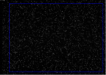
[06-AUG-18] As we present below, our image sensors are sensitive to x-rays. For a dose rate of 440 mR/min measured with our ionization chamber, we obtain charge density 0.27 counts/pixel in a TC255 with 100-ms exposure. The charge density increases linearly with dose rate.
[06-DEC-12] We use our Pulsed X-Ray Source and our Radcal Ionizing Chamber to calibrate the response of a TC255P Dosimeter to x-rays of average energy 27 keV and maximum energy 60 keV. As we show elsewhere, our pulsed x-rays deposit roughly 7.3 times as much energy in silicon as they do in air, so a 1-R dose is equivalent to 64 mGy in Si. We use this conversion factor to determine the sensitivity of our image sensor to ionizing energy deposition.
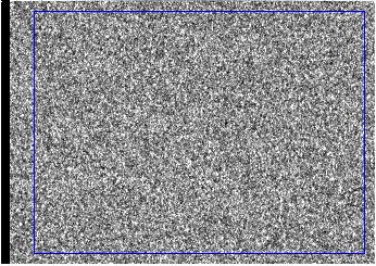
We use our ionizing chamber dosimeter to determine the dose at a point in the x-ray beam 50 cm from the source. We measure 205 mR in one second and 20.0 mR in 0.1 s. In units of Gy in Si, these doses are 13 mGy and 1.3 mGy respectively. We place the TC255P at this location, with its image plane perpendicular to the x-ray beam, and expose it to x-rays with the help of the Dosimeter Instrument. We vary the dose by varying the pulse time and the image sensor exposure time with a Toolmaker script, DSM_1. The following image we obtained with a 1-s exposure, or 205-mR dose.
At each dose we measure the average charge deposited by x-rays in the image pixels. The Dosimeter takes two images, one with the dose, and one without the dose, and subtract them to remove the background intensity due to electronic offsets. We specify a threshold of two counts for charge detection. The Dosimeter obtains its charge density measurement in the following way. Any pixel with intensity greater than the threshold will have its net intensity above threshold added to the total image charge. We divide by the number of pixels in the analysis boundaries and so obtain the charge density in counts/pixel. We begin by increasing the pulse length from zero in 50-ms steps to 1000 ms.
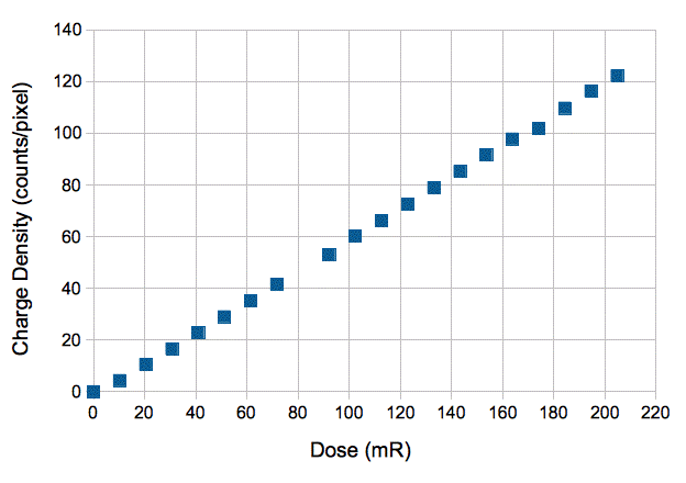
We fit a straight line to the above graph and obtain a slope of 614 counts/pixel/R, or 9.6 counts/px/mGy. We repeated our experiment, but using the TC255P image area pixels rather than the light-shielded storage area pixels. We turned off the overhead lights and placed tape over the sensor. We obtained a slope of 668 counts/pixel/R, suggesting that the image area pixels are slightly deeper than the storage area pixels. We rotate the sensor so that it's image plane is parallel to the x-ray beam. The x-rays are now moving from right to left in the image. We obtain the following 10-ms exposure that shows individual x-ray hits.
With the sensor rows parallel to the x-ray beam, electrons ejected by interactions with the x-rays will tend to move from right to left more than in other directions. The hits remain isolated to one or two pixels, with no apparent bias towards spreading in the row direction. We conclude that the electrons ejected by our x-ray beam travel no more than a few microns through silicon, which is consistent with our discussion above. We repeat our sensitivity experiment, going from 0 ms to 100 ms, and obtain a sensitivity of 42 counts/px/R. We rotate the sensor so that it is 45° to the beam, and obtain sensitivity 0.479 counts/px/mR.
We insert a 13-mm Al absorber in front of the x-ray source. Our ionizing chamber records a new dose rate of 15.7 mR/s. The absorber eliminates almost all x-rays below 10 keV, and our source cannot produce x-rays above 60 keV, so we know our spectrum now lies within the range 10-60 keV. We obtain the following image with a 10-ms exposure.
We increase the pulse length from 0 ms to 500 ms in 10-ms steps to obtain the TC255P response to the spectrum of x-rays that emerges from our 13-mm Al absorber.

We fit a straight line to the above graph and obtain a slope of 523 counts/px/R or 8.2 counts/px/mGy. The residuals to the fit are parabolic with standard deviation 0.068 counts/pixel, suggesting linearity to 0.13 mR.
We move the image sensor, with the 13-mm absorber in place, to a range of 200 cm. Our ionizing chamber records a dose rate of 1.00 mR/s. We repeat increase exposure time from 0 ms to 100 ms in 10-ms steps. We obtained a slope of 376 counts/pixel/R. The residuals to our fit are 0.002 counts/pixel, so our dose resolution is 6 μR, or 400 nGy in Si.
At 50 mR the storage area pixels of the TC255P have sensitivity to x-rays of 614 counts/px/R, at 5 mR their sensitivity is 523 counts/px/R, and at 50-μR their sensitivity is 376 counts/px/R. The sensitivity is lower at low dose rates because the intensity threshold we use in our charge-counting calculation is more significant when compared to the charge deposited by the low dose of x-rays.
[10-DEC-13] We sent our Radcal meter back to the manufacturer for repair and re-calibration in September 2013. We have it back now and we use it to calibrate two image sensor dosimeters. We place the ionization chamber, a TC255P, and an ICX424 image sensor 200 cm from our pulsed x-ray source. We generate pulses of x-rays with a 70-keV anode voltage and record the Radcal dose. We increase the pulse length from 0 ms to 1000 ms. Later, we generate pulses with the lights off and use the image area of a TC255P and an ICX424 to detect the x-rays. For each pulse, we expose the image sensor for 2000 ms, which is sufficient time to accommodate the longest pulse (1000 ms) and the x-ray set-up and switch-off times (650 ms combined). The two-second exposure causes dark current and background light to increase the average intensity of the ICX424 image from 32 counts to 38 counts, and that of the TC255P image from 48 counts to 98 counts. We set the threshold for charge density measurement at 42 counts for the ICX424 and 102 counts for the TC255P. We obtain the following graphs with the help of the DCM_2 Toolmaker script.
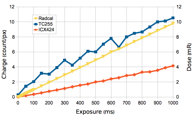
We ran this experiment remotely from our home seven miles from the apparatus. The large deviations from a straight line that we see in the TC255P data are stochastic. We believe they are due to fluctuations in the image download time, which affects the dark current accumulated by the sensor. Using the slopes of these graphs, the sensitivity of the TC255P is 975 counts/R and of the ICX424 is 417 counts/R. The TC255P image area pixels are 10 μm square, and those of the ICX424 are 7.4 μm square.
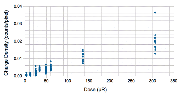
[11-DEC-13] We have our two image sensor dosimeters and our Radcal ionizing chamber arranged as yesterday, but now 100 cm from the source. We set the pulse length to 500 ms and introduce aluminum absorbers of increasing thickness, with the help of aluminum foil sheets and aluminum plates. We obtain the following graphs of charge density and dose versus aluminum thickness.

For each absorber, we pulsed the x-ray once for each image sensor and accumulated the dose of both pulses in the Radcal ionizing chamber. The plot gives the dose for both pulses and the charge density in each sensor. We exposed the image sensors for two seconds each time. The ICX424, with its much lower dark current, is able to measure lower doses than the TC255P.
[12-DEC-13] We set up our TC255P and ICX424 dosimeters at range 100 cm, and the Radcal ionizing chamber beside them. We produce x-rays with our Continuous X-Ray Source. We add absorbers and measure the dose rate and our image sensor charge density. At each absorber depth, we turn on the source, which takes sixty seconds, and use our DSM_3 script to expose the image area of each CCD for half a second, record the Radcal dose rate, and turn the source off. We obtain the following graph.

To obtain the charge density, we measured the average intensity of the CCD images for 0.5-s exposures in the darkened room and no x-rays. We added two counts to this average to obtain the threshold for charge measurement. When we start with aluminum foil sheet absorbers, the Radcal dose rate drops significantly with each added sheet, but the TC255P and ICX424 dose rate remains unchanged. The Radcal ionizing chamber has a 1.0-mm wall of polycarbonate. The TC255P and ICX424 have glass windows 0.75 mm thick. Most x-rays above 7 keV, but very few below, will penetrate the Radcal chamber. Most x-rays above 14 KeV will penetrate the glass window, but very few below. The 0.13-mm thick beryllium window of our continuous source allows most x-rays above 2.5 keV to pass through, but very few below. An aluminum absorber of 0.3 g/cm2 allows most x-rays above 14 keV to pass through, but very few below. For aluminum absorbers less than 0.3 g/cm2, x-rays between 7 keV and 14 keV will pass through and be recorded by the Radcal but not the image sensors. Once we have more than 0.3 g/cm2 of aluminum absorber, the TC255P, ICX424, and Radcal observe the same attenuition from further absorbers, because the dose consists of x-rays above 14 keV.
The Dosimeter Instrument allows us to use image sensors to take x-ray images. The following image we took with the Dosimeter and a phosphor-coated KAF0400. The Dosimeter clears the image sensor, sends a command to a pulsed x-ray source, and reads out the sensor. The figure below shows a contact print of a printed circuit board taken with a phosphor-coated image sensor and our Continuous X-Ray Source.
We see a via in a 1.6-mm thick printed circuit board, and a 34-μm thick copper track. The phosphor is 34 μm deep. All our image sensors will take x-ray images, but the most sensitive sensors are those with a coating of phosphor. We have KAF0400 image sensors with phosphor coatings up to 120 μm thick. These offer over ten times the sensitivity to x-rays as our bare image sensors. But the thicker the phosphor, the more the blurring of the image lines as light from the top of the phosphor spreads out on its way to the silicon surface of the image sensor.
[15-MAR-12] We use a calibrated, portable Cs-137 gamma source to measure the sensitivity of TC255P pixels to gamma rays. The source strength is 0.123 μRm2/s. We multiply by exposure time and divide by the square of the range to obtain the dose in μR. The Cs-137 decay almost always produces an electron of energy 510 keV and a photon of energy 660 keV. The electron is absorbed in the material around the source, leaving the photon as the only emerging product. We obtained the following TC255P image with a 1-s exposure at range 50-mm. The expected dose is 50 μR.
By changing the range of the source and measuring image charge density multiple times at each range, we obtained the following graph of TC255P image charge density versus dose in Roentgen.
The slope of the graph is 0.0658 counts/px/mR. This is the response of our TC255P to 660-keV photons. Its response to 10-60 keV photons is 0.523 counts/px/mR, as we showed above. In the range 10-60 keV, the energy absorption coefficient of silicon is seven times greater than that of air. But at 660 keV the coefficients are almost the same. The Roentgen is a measure of charge deposition in air. One Roentgen is 0.258 mC/kg in air, which implies 8.77 mJ/kg of energy deposited in air. Radiation consisting of 660-keV gammas will deposit the same amount of energy per kilogram in air and silicon. But 30-keV x-rays will deposit 7.6 times as much energy per kilogram in silicon as in air. Thus we expect our TC255P sensor to be 7.6 times more sensitive to x-rays than gamma rays. Here we see a sensitivity ratio of 0.523 / 0.0658 = 7.9.
[15-APR-14] We obtain the following ICX424 image in a cesium-137 irradiation chamber, as described here. The expected dose at the image sensor is 8.1 R/min. Exposure time is 50 ms. Readout time is 40 ms, but the readout array in the ICX424 is an order of magnitude less sensitive to ionizing radiation than the image area. So the effective exposure of the pixels remains 50 ms, which means they are subject to an average dose of 6.8 mR.

The charge density in the ICX424 image is 0.22 count/px. If we trust the 8.1 R/min dose rate given by the chamber manufacturer, and convert to Gy with 0.00877 Gy/R, we get sensitivity 0.051 count/px per Gy/hr.
In the ATLAS experiment, we expect the background ionizing radiation to be dominated by 200-keV to 1 MeV gamma rays. As we increase the luminosity and beam energy, the dose rate should increase in proportion to both, but the spectrum of the radiation will remain the same. We would like to use our image sensors to measure dose rate in our radiation tolerance tests, and also perhaps in the ATLAS experiment itself, as an independent measurement of the background rate. But we do not have a continuous and intense source of ATLAS-like gamma rays with which to irradiate our electronics. We have x-ray sources, both pulsed and continuous.
We calibrate our image sensor dosimeters with x-rays and an ionizing chamber dosimeter. The ionizing chamber dosimeter tells us the charge charge deposited per kilogram in air (Roentgen) by the x-ray dose. We convert this to energy deposited per kilogram in air (Gray in air) using the ionization energy of air. We convert this to energy deposited per kilogram in silicon in two steps. First, we measure the spectrum of our x-ray source with the help of various absorbers. Second, we use the energy-dependent absorption coefficient of air and silicon to determine the amount of energy that would be deposited in silicon by a dose that deposits 1 J/kg in air (1 Gy in air). Thus we determine the response of the image sensor to energy deposited per kilogram in silicon.
This calibration at first appears daunting, because the absorption coefficients of all materials vary dramatically from 1 keV to 100 keV. But it turns out that between 2 keV and 60 keV, the energy absorption coefficient of air, is roughly seven times lower than that of silicon. Because our x-ray energy spectrum lies between 2 keV and 60 keV, we can simply multiply Gray in air by 7.0 to obtain Gray in silicon. At energies above 200 keV, the absorption coefficients for air and silicon are very close to one another, so we can muliply by 1.0 to convert between the two. The ATLAS ionizing radiation doses are given in Gray without specifying silicon or air, and this is because it makes no difference whether the absorbing material is silicon or air when the dose is made up of gamma rays
For doses of order 1 mGy in Si (0.1 rad in Si), our TC255P dosimeter has sensitivity 8.5 counts/px/mGy. It is linear with dose to within a few percent. It responds to pulses of radiation from a 1 μGy to 10 mGy, and it can measure dose rates as low as 1 μGy/s.
In addition to being ionizing dosimeters, our image sensors have a chance of monitoring the accumulated fast neutron dose during the experiment. This measurement may be possible because we know the temperature of the sensors to within 0.1°C, so we can account for temperature when measuring the increase in dark current that is created by fast neutrons.