Camera Head (A2075) Manual
© 2012-2018, Kevan Hashemi, Brandeis University
© 2022-2024, Kevan Hashemi, Open Source Instruments Inc.
Contents
Description
Versions
Operation
Image Geometry
Optical Response
Sensor Details
Electronics
Development
Description
The Camera Head (A2075) is a LWDAQ Device that controls and reads out a single ICX424 image sensor. The circuit provides a socket into which we can solder the sixteen-pin sensor directly. It provides a twelve-way flex socket to which an auxiliary board holding the sensor can be connected. Connect only one sensor at a time.

Figure: Camera Head (A2075B) with Cover Removed. An ICX424AL monochrome image sensor is on the right side, beneath a DSL821 lens in a CMT821 M12×0.5 lens holder. The layout of the circuit is spacious, and provides both a footprint for an image sensor and a connector for an external image sensor. The square chip near the center is the programmable logic. The enclosure is a plastic PPL.
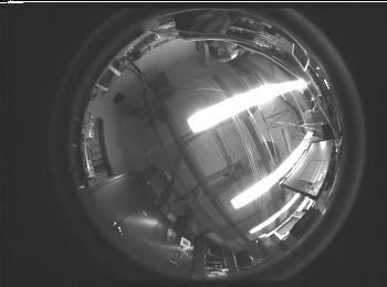
For a photograph of an ICX424AL sensor see here. Below is an image we obtained with an ICX424AL monochrome image sensor and our A2075A prototype circuit board.

Figure: Fish-Eye View. This image taken with a DSL216A fish-eye lens, ICX424AL monochrome image sensor, and exposure time is 20 ms. The image is not intensified. It consists of 520 rows and 700 columns.
In the example image, the over-head lights saturate the image pixels. Even if we divide the exposure time by a factor of a hundred, they still saturate the image pixels. And yet we see hardly any spread of this saturating charge into neighboring pixels. (The spread is called blooming, and the ICX424 provides automatic anti-blooming.) When we block light to the sensor, the noise we see in the image is around 0.2 counts, which is what we expect from quantization (1/√12). With a 1-s exposure in the dark, we see no more than a few counts increase in the background intensity, which suggests we can expose with the ICX424 for many seconds at room temperature.

Figure: Fish-Eye View, Quadruple-Pixels. We combine blocks of four pixels with vertical and horizontal binning. The image consists of 260 rows and 350 columns. Each pixel corresponds to one 14.8 μm × 14.8 μm pixels in the image sensor. Exposure time is 5 ms. We display the image without intensification.
By combining rows and columns into pairs within the image sensor at the time we read out the image, we can create an image with pixels four times the size. The image above is such an image, but we display it with the same screen pixel size, so it appears to be one half the width and one half the height. Notice that despite the fact that the exposure time is one quarter that of our full-size image, the contrast and brightness are roughly the same. This is because we are combining the charge from four pixels together into one output pixel.

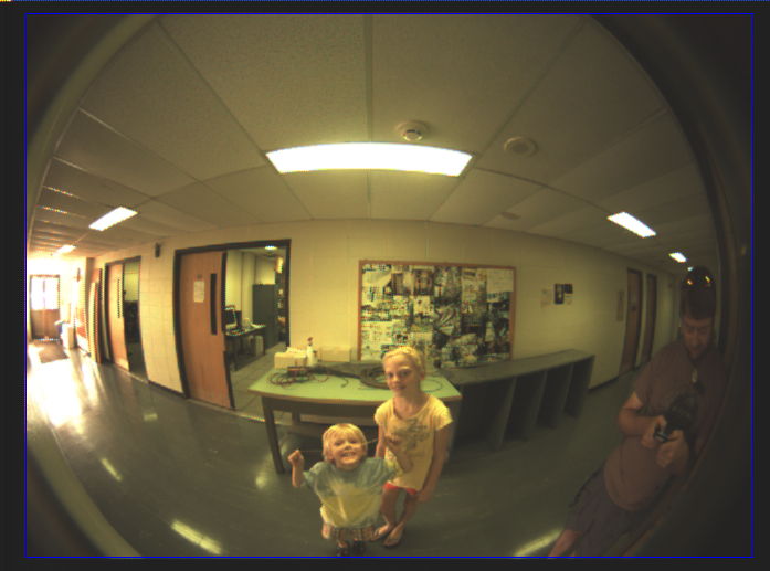
Figure: Color Image. Taken with a DSL215 fish-eye lens, ICX424AQ color image sensor, 40 ms exposure time, and rggb image intensification.
The ICX424AQ is a color mosaic image sensor we can read out with the same process as the monochrome sensor. When we display the full-size image in our LWDAQ software, we use one of the LWDAQ color mosaic image intensification options, such as rggb. The color mosaic used by the ICX424AQ follows the same pattern used by the TC236P (see here). The "rggb" in the name of the intensifiction tells the display routine to divide the image into four-pixel squares, in which the top-left pixel is red, and the bottom-left is blue, with the other two being green. The ICX424AQ is approximately half as sensitive to light as the ICX424AL. This decreased sensitivity is a consequence of its color filters.

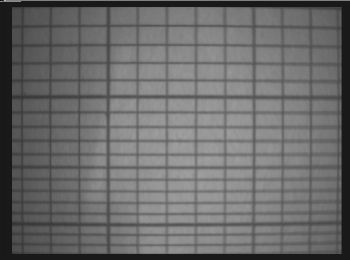
Figure: Barrel Distortion. Lines are bent away from the center. The object is logarithmic graph paper 50 mm from a DSL821 lens, which is in turn 7 mm from the image plane. The DSL821 is a compound lens with an aperture. Whenever the aperture is separated from the lenses by a distance that is significant compared to the focal length, we expect to see either barrel or pin-cushion distortion. The fact that we see barrel distortion suggest that the aperture towards the front of the compound arrangement. We do not expect such distortion in a BCAM, where our aperture is only 1 mm behind a lens of focal length 50 mm or 75 mm.
If we take a quadruple-pixel image with the ICX424AQ color mosaic sensor, we end up combining blocks of four pixels together into one. Each block of four pixels contains one red, two green, and one blue pixel. The combined result is a single, quadruple-size monochrome pixel with half the sensitivity of the quadruple-size ICX424AL monochrome sensor. Thus we can use the quadruple-size readout with a color mosaic sensor, and obtain a monochrome image. But we cannot use the full-size readout with the color mosaic sensor to obtain a monochrome image, nor can we use the quadruple-size readout to obtain a color image.
Versions
We define the following versions of the A2075. Some have the sensor loaded on the circuit board, others do not. Some have a control signal from the logic chip to the sensor flex socket. Pin U5-47, shown as TP1 on the schematic, is connected to J2-11 through a resistor R44. We load R44 with a resistor to complete the connection. The control signal is a 3.3-V logic level we can use on the ICX424 Minimal Head to flash light sources.
| Version | PCB | Description |
|---|
| 2075A | A207501A | Camera Head Prototype |
| 2075B | A207501B/C | Laboratory Camera, Monochrome, PPL Enclosure |
| 2075C | A207501B/C | Laboratory Camera, Color, PPL Enclosure |
| 2075D | A207501D | LGT Centering Camera, NS |
| 2075E | A207501C | Chamber Rasnik Head, NS, CS |
Table 1: Versions of the Camera Head (A2075). NS = No Sensor on Circuit Board. CS = Control Signal for Minimal Head.
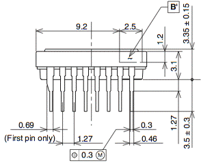
The ICX424 is one of Sony Semiconductor's Progressive Scan System CCDs. It comes in two packages, a 14-pin round ceramic DIP (see DIP14) and a 16-pin rectangular DIP (see DIP16). The sensor comes comes in a monochrome version and a color mosaic version. The ICX424AL is the 16-pin monochrome, and the ICX424ALB is the 14-pin monochrome. The ICX424AQ is the 16-pin color mosaic, and the ICX424AQB is the 14-pin monochrome. We built our first prototype with the 16-pin monochrome in the 16-pin package. The 16-pin package is 11.6 mm × 11.4 mm, while the 14-pin package is a square 9.5 mm on each side, with the corners rounded off on a 5-mm radius.
The A2075A provides a footprint for the 16-pin package, but we can drive the 14-pin package through J2, the 12-way, 1-mm flex socket. Resistor footprints R38 and R39 allow us to hard-wire one of the two possible sensors to the output amplifier of the A2075. If we connect an external sensor, we remove R39, which is a 0-Ω solder lump, and put a 0-Ω connection in place of R38. The 14-pin package is significantly smaller, but Sony informs us that it is intended only for medical purposes, and is substantially more expensive than the 16-pin device. Thus we have no plans to use the 14-pin devices.
The A2075D does not have a sensor on board, but instead connects to an auxiliary sensor head such as any version of the A2076. The circuit is missing some parts called for on the page three of the schematic. The missing components are U11, C9, C10, C11, R39, and R38.
The A2075E provides an additional signal on J2 to turn on and off a light source on an ICX424 Minimal Head such as the A2076G. Resistor R44 with value 0.0 Ω connects TP1 to J2-11. The control signal is 0.0 V by default, but becomes 3.5 V when we set device command bit DC10.
A close relative of the A2075 is the BCAM Head (A3025), which provides connection to two external image sensors and switches for six external light sources.
Operation
The A2075 is a LWDAQ device of type ICX424 (6) when we read it out one pixel at a time, and device type ICX424Q when we read it out with quadruple pixels. The A2071E and A2037E LWDAQ Drivers support both device types, but you will need firmware version 2+ for the A2071E and 15+ for the A2037E.
The A2075 command bits are assigned as follows. The assignment conforms to the LWDAQ Specification for device types ICX424 and ICX424Q, but does not include the bits that turn on and off light sources or select a second image sensor, because there are no light sources on the A2075, and we select the external image sensor with jumpers on the circuit board (R38 and R39).
| DC16 | DC15 | DC14 | DC13 | DC12 | DC11 |
DC10 | DC9 | DC8 | DC7 | DC6 | DC5 |
DC4 | DC3 | DC2 | DC1 |
|---|
| PXBN | X | X | X | X | X |
ON1 | X | WAKE | LB | SUB | V3 |
V2 | V1 | H | RDP |
Table 1: Command Bit Allocation of the A2075. An "X" means the command bit serves no function.
The ON1 bit is implemented in the A2075E to flash a light source on the ICX424 Minimal Head through J2. Use the flash job in the LWDAQ Driver to flash the light source. Specify source device element one (1) and source device type IXC424 or ICX424Q (6 or 7).
The RDP bit, when combined with V2 and V3, causes a read pulse to be administered to the image sensor, transferring charge from the image area to the transfer columns. The H bit enables the horizontal clock phase in the circuit. The V1, V2, and V3 bits control the image sensor's vertical clock phases. The SUB bit causes a substrate pulse to be administered to the image sensor, clearing charge from the image area. The WAKE bit turns on the ±15V power supplies to the image sensor circuit and LB enables loop back for the measurement of cable propagation time. The PXBN bit selects pixel binning, which combines each block of four pixels into one.
The V1, V2, V3, SUB, and RDP bits allow the LWDAQ Driver to clear, expose, and transfer image rows into the sensor's output register. The driver manipulates these bits with a combination of command transmissions controlled by the LWDAQ Software and command transmissions that it performs as part of device-dependent jobs. The following lines are taken from the Camera Instrument in LWDAQ 8.2 and later. As we explain later, the ICX424 has a separate array of readout pixels. If we allow more than a few seconds to pass since our last image readout, dark current and noise will accumulate in these readout pixels, so we must clear them of charge. We do this with a move job. We clear the image pixels with a single pulse on the substrate clock. We time the exposure with the driver's delay job.
# Clear the vertical transfer columns with a move job.
LWDAQ_execute_job $sock $LWDAQ_Driver(move_job)

# Clear the image area with a substrate pulse. We set
# V2 and V3 hi and V1 lo to keep charge constrained in the
# vertical transfer columns.
LWDAQ_transmit_command_hex $sock 0098
LWDAQ_transmit_command_hex $sock 00B8
LWDAQ_transmit_command_hex $sock 0098

# Expose image area.
LWDAQ_delay_seconds $sock $config(daq_exposure_seconds)

# Transfer the image out of the image area and into the
# transfer columns by applying read pulse to V2 and V3.
# We keep V1 lo to maintain pixel charge separation in
# the vertical transfer columns.
LWDAQ_transmit_command_hex $sock 0099
LWDAQ_transmit_command_hex $sock 0098

# Drive V2 hi, V1 and V3 lo so as to collect all pixel
# charges under the V2 clock.
LWDAQ_transmit_command_hex $sock 0088
Now that we have the image charges in the readout pixels, we move the image rows down into the output register one by one, clock the individualt pixels out one by one, digitize their intensities, and store them in the driver's memory. This we do with a read job applied to the ICX424 device, for single pixels, or the ICX424Q device for quadruple pixels.
# Transfer the image to driver memory with the read job.
LWDAQ_set_data_addr $sock 0
LWDAQ_execute_job $sock $LWDAQ_Driver(read_job)
During the read job, the driver moves one row at a time into the output register. It does this by sending command so the A2075 that manipulate the vertical clock phases, V1, V2, and V3.Once it has moved a fresh row into the output register, it sets the H bit. This bit enables the driver to control the output register's H1 and H2 clock lines directly with the LWDAQ transmit signal, which appears as A in the schematic. The driver transmits a series of stop bits to clock the output register pixels into the output transistor.
If we use the ICX424Q device type for the read job, the driver will combine pairs of rows in the output register, and it will set the PXBN bit for the A2075. The output register does not have a V1 phase, so that the charge that exists already in the register remains there during further downward shifts of the image rows. Thus combining rows is simply a matter of moving the image down by two rows, because this combines the charge of both rows in the output register. With the PXBN bit set, whenver the A2075 programmable logic sees a new LO pulse on A, it generates two LO pulses on H1 and two HI pulses on H2 so as to move two output register pixels into the output transistor. Thus the driver combines two rows and the A2075 combines two columns. The result is quadruple-sized pixels. We discuss the details of the double-clocking of the image sensor here.
Our next step is to transfer the image from the driver to our computer, which we do as follows.
# Send the device to sleep, read the image out of the
# driver, and close the socket.
LWDAQ_sleep $sock
set image_contents [LWDAQ_ram_read $sock 0 $image_size]
The Camera Instrument provides buttons that configure them for the TC255, TC237, KAF0400, ICX424, and ICX424Q device types. The configuration sets the device type, the image width and height, and the analysis boundaries so that we will obtain correct readout and intensification of images. The BCAM and Rasnik Instruments provide the same buttons, but in the Info Panel rather than on the main instrument panel.
Image Geometry
[14-JUN-24] On the screen of our computer, where our LWDAQ program displays the images we acquire from the ICX424AL, we plot the first pixel we obtain from the sensor on the top-left. Subsequent pixels form the first row from left to right. Subsequent rows fill in the image from top to bottom. In our image analysis code, we use x for the horizontal image coordinate, and y for the vertical. Our origin is at the top-left corner of the top-left pixel. Thus x is left to right in the image and y is top to bottom.
The following annotated photograph shows how x and y from the image display correspond to the layout of pixels on the image sensor itself. The first pixel we read out is the one on the top-left in the photograph, which is the one nearest to pin nine of the sixteen-pin package.

Figure: Image Geometry for the ICX424.
The ICX424 pixels are each 7.4 μm square. The image we obtain from the LWDAQ hardware has 700 columns and 520 rows. Thus the image corresponds to a physical area 5.180 mm × 3.848 mm. We note that this ICX424 geometry is similar, but not identical to the geometry of our TC237B readout. The TC237B pixels were also 7.4-μm square.


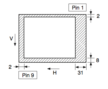
Figure: ICX424 Dark Pixels and Pin One Location. Both drawings from the ICX424 data sheet. The V and H arrows show the direction of movement of pixels during readout. The first pixel to be read out is the one next to pin 9. We identify pin 1 by looking for its unique pin shape, as seen on left end of package in the drawing.
As shown above, the ICX424 provides dark columns and rows around the image area. These dark pixels provide us with a border around the light-sensitive area, and give us pixels that we know are black. Our LWDAQ readout adds and subtracts some rows and columns, so that the actual dark border in a displayed image is slightly different from the border on the sensor itself.
| Parameter | Value | Description |
|---|
| daq_device_type | 6 | Specifies ICX424 device for LWDAQ firmware |
| daq_image_height | 520 | Number of rows |
| daq_image_width | 700 | Number of columns |
| daq_image_left | 24 | Left edge of active area |
| daq_image_top | 14 | Top edge of active area |
| daq_image_right | 682 | Right edge of active area |
| daq_image_bottom | 506 | Bottom edge of active area |
Table: Single-Pixel ICX424 Analysis Boundaries and Image Dimensions for LWDAQ Instruments.
The LWDAQ readout of the ICX424 provides 23 dark columns on the left and 17 on the right. There are twelve dark rows at the top and 12 on the bottom. When we need to specify the center of the image area, as we do for Rasnik Analysis and BCAM Analysis, we use the point that lies at the exact center of the image as it appears in the LWDAQ readout. The coordinates of this point, in microns from the top-left corner of the image, are x = 2.590 mm and y = 1.924 mm.
When we read out the sensor with vertical and horizontal pixel binning, we end up with pixels that contain charge from four original image pixels. These are quadruple pixels, and we need a new device type and dimensions, as shown below.
| Parameter | Value | Description |
|---|
| daq_device_type | 7 | Specifies ICX424Q device for LWDAQ firmware |
| daq_image_height | 260 | Number of rows |
| daq_image_width | 350 | Number of columns |
| daq_image_left | 12 | Left edge of active area |
| daq_image_top | 7 | Top edge of active area |
| daq_image_right | 341 | Right edge of active area |
| daq_image_bottom | 253 | Bottom edge of active area |
Table: Quadruple-Pixel ICX424Q Analysis Boundaries and Image Dimensions for LWDAQ Instruments.
You can set up the Camera Instrument with either of the above geometries by pressing its ICX424 or ICX424Q buttons (you will need LWDAQ 7.7 or later). If we calibrate a camera with single-pixel readout, and subsequently operate the camera with quadruple-pixel readout, we can transform feature positions in the quadruple-pixel image into feature positions in the single-pixel image so as to apply the single-pixel calibration constants. We add 44.4 μm to the x-coordinate and 7.4 μm to the y-coordinate we obtain from quadruple-pixel readout and so obtain the feature position in a single-pixel image captured from the same sensor. We measure the offset between quadruple and single pixel image positions here.
The surface of the image sensor is 1.94 mm from the surface of the glass. The glass itself is 0.75 mm thick. We assume the glass has a refractive index of roughly 1.5. The optical depth of the image area from the surface of the glass will be (1.94 mm − 0.75 mm) + (0.75 mm ÷ 1.5) = 1.69 mm. The package height is 3.35 mm, so if we press the package right down onto the printed circuit board, the optical location of the image area will be 1.66 mm from the printed circuit board.
The ICX424 comes in a color version also. The monochrome part is the ICX424AL and the color mosaic part is the ICX424AQ. The color mosaic places blue, green, and red filters over alternating pixels, and so allows us to deduce the color of the light incident upon the sensor. To render the color image from such a sensor on the screen, we use the rggb types of image intensification.
Optical Response
The ICX424AL data sheet does not specify the pixel capacity in terms of electrons, nor does it specify the sensor's quantum efficiency. But it does contain this graph of relative spectral response. The fact that the sensitivity at 400 nm (violet) is 60% of the sensitivity at 500 nm (green) suggests that the sensor is a back-illuminated CCD, meaning the top side is a polished piece of silicon, and all the clock lines, and readout features are on the dark side. We are not certain this is the case, but if so this would mean over 95% of each pixel is sensitive to light, and 90% of light penetrates to the sensitive region of the sensor.

Figure: Spectral Sensitivity of the ICX424AL.
Image pixels can hold only a certain number of electrons before these electrons, by their own negative charge, begin to repel one another and spread out of the pixel. This spread of charge tends to occur most in the column direction of traditional CCDs, but the ICX424 almost entirely eliminates this spread of charge with the use of potential wells around the edges of the pixels, which accept overflowing electrons and remove them from the sensor. One question that arises with any image sensor is how the saturation of the pixels will affect the linearity of its response.
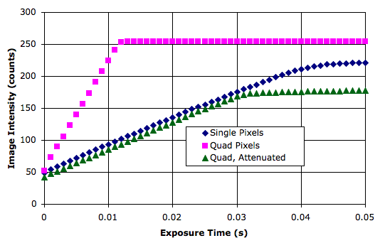
We covering the sensor with a piece of card and exposing it for increasing intervals. We measured the average intensity of the light-sensitive portion of the image. The blue points in the following figure show how the intensity increases with exposure time. We see the intensity starting to flatten out at around 35 ms, and we see the saturation intensity is around 220 counts. The linearity of the response from 0 to 30 ms is 1.5%.

Figure: Linearity of Response.
When we combine four pixels into one, with horizontal and vertical binning, we naturally end up with four times as much charge in each pixel of the output row. The pink points show how the image intensity with the quadruple pixels varies with exposure time. We reach the saturation voltage of our ADC at 12 ms, and see no sign of saturation of the output register pixels. The linearity of the response from 0 ms to 10 ms is 2.0%. We attenuated the output of our A2075 by a factor of 3.5 and repeated our measurements. We obtained the green points.
The attenuated quad pixel output saturates at around 170 counts with a 30-ms exposure. Linearity from 0 ms to 30 ms is 0.7%. If the output register pixels had infinite capacity, we would expect four saturated image pixels to produce an output of 220 × 4 ÷ 3.5 = 250 counts. But saturation occurs at 175 counts. Thus we conclude that the output register pixels have saturation capacity roughly three times that of the image pixels, but not quite four times.
The sensor data sheet gives the linearity at 1%. We have no reason to doubt them. Even a linearity of 5% would be adequate for our Rasnik and BCAM instruments, as well as video cameras.
Sensor Details
The ICX424 data sheet does not present the detailed structure of the sensor. Nevertheless, the data sheet combined with our own tests together give us enough indirect information to make an educated guess as to how the sensor is built and how it works. Here we describe how we clear, expose, and read out the image sensor, and we present our best guess as to how the sensor is built.
The sensor is a piece of silicon. Photons arriving in the silicon are absorbed and generate electron-hole pairs. The slicon must be equipped to constrain these electrons so that they stay near the place they were generated. Vertical and horizontal features will divide the sensor into squares called pixels. Charge generated in each pixel will remain separate from charge generated in other pixels. We must have some means to clear all existing charge out of all the pixels, so that we can begin a new exposure. And we must have a way to extract each of the pixel charges so as to measure them and so create our digital image.
We begin with a flat piece of silicon, which we call the substrate. We dope the top surface so that it is N-type. This creates a depletion region a little distance into the silicon, and within this layer there is a maximum in electrical potential, just inside the N-type material. Electrons generated in the depletion layer move towards this maximum, while the holes move away. The electrons remain trapped in the depletion layer, while the holes move away from it. We add thin vertical and horizontal lines of P-type doping, so as to create a grid of negative potential wells. We call these band stops. They define the borders of our pixels. Holes reaching the top surface move towards the band stops and disappear into them. Electrons, however, are repeled by the band stops, and so remain trapped within their pixels.
Judging from its spectral sensitivity, the ICX424AL is a back-illuminated CCD. Light enters the bottom of the substrate. The substrate is connected to a substrate clock input, and a sufficiently high potential on this input will suck the electrons out of the depletion region of each pixel. This is what we are doing when we apply a 22.5-V pulse to the substrate pin of the ICX424AL. The sensor generates its own 9-V substrate bias and we apply a 22.5-V pulse through a capacitor to the sensor's substrate pin. The A2075 circuit creates a 22.5-V pulse by driving the output of an op-amp from −7.5 V to +15 V. When we apply this pulse to the substrate pin through a 100-nF capacitor, we see the substrate voltage go from 9 V to 31.5 V.
The ICX424 pixels are, however, more complex than we have described so far. We have not yet considered the manner in which we can transfer the pixel charges out of the image sensor. The ICX424AL allows us to transfer all the pixel charges into readout columns, and then to transfer the pixels down the readout columns like packets of charge down a conveyor belt. The sensor allows us to perform this transfer even as we are exposing the pixels to more light and so creating our next image. Furthermore, the light falling on the sensor does not affect the charge being transferred.
Because the sensor is back-illuminated, we can deposit further layers of metal, glass, and polysilicon on top of the substrate, without having to worry about stopping light from penetrating to the heart of the pixel. The light enters through the other side of the pixel. The ICX424 manages to create another array of pixels, which we call the readout pixels in the shadow of a reflecting metal layer, on top of the substrate. Horizontal conductors run across the width of the image sensor, defining the row direction, and making capacitive contact with the readout pixels. There are three such conductors per pixel. The conductors are connected at the edges of the sensor into three sets: V1, V2, and V3. When we apply +15 V to V2 and V3, with −7.5 V on V1, charge moves from the image pixels into the readout pixels, where they are in the shadow of an aluminum barrier. They are no longer affected by light landing upon the sensor. Nor are they affected by the substrate pulse. We can clear the image pixels with a substrate pulse at any time, and the readout pixels will be entirely unaffected.
When V2 = 0 V and V1 = V3 = −7.5 V, the readout pixel charges gather beneath the V2 conductors. When V2 = V1 = 0V and V3 = −7.5 V, the charge spread out beneath V1 and V2. When V2 = V3 = −7.5 V and V1 = 0 V, the charge gathers under V1. And so we see that we can move the charge from V2 to V1 to V3 to V2, and so on, and so take the charge from one readout pixel and move it to the row below, and continue doing this until all the pixel rows have been moved out of the bottom row of the image. When a row moves off the bottom, it enters the output register. The output register is equipped with two clock conductors per pixel, called H1 and H2. As we go from right to left along the row, we encounter H1, H2, H1 and so on. In addition to its three vertical transfer clocks, the output register row has two horizontal transfer clocks. Each readout pixel is equipped with potential wells that allow us to transfer pixels from from right to left along the row simply by alternating 0 V and +5 V on H1 and H2. When we transfer a row of pixels into the output register, we hold H1 at 0 V and H2 at +5 V. We switch the voltages and one of the pixels comes out of the left end of the output register.
The electrons of this pixel, leaving the output register, arrive at the gate of the sensor's output transistor. The voltage at the drain of the transistor, which is the sensor output, drops in proportion to the total charge deposited upon its gate, which is proportional to the light received by the original image pixel. The sensor output is now at the pixel level. We clear charge from the output transistor gate by applying to it a reset pulse. The reset pin of the sensor provides a reset bias of 12 V and we apply a 5-V pulse to this pin through a capacitor. In the A2075, we generate the 5-V pulse with an op-amp and pass it through a 100-nF capacitor to the sensor reset pin. The result is a 17-V reset voltage on the gate of the sensor's output transistor (12 V + 5 V = 17 V). After this pulse, the gate of the output transistor is cleared of pixel charge. The sensor output moves to its black level. When we read out the ICX424 with the A2075A, the LWDAQ Driver subtracts the black level from the pixel level to obtain a voltage proportional to the light that landed upon the image pixel. The LWDAQ Driver digitizes this voltage with 8-bit precision and stores the result in its memory.
We apply another clock cycle to H1 and H2, and the next time H1 0 V, the next pixel charge arrives at the output gate. In this way, we read out each pixel in turn. Each ends up as an eight-bit number in the LWDAQ Driver memory. If we refrain from reseting the output gate, it turns out that we can add the charge of the next pixel to the charge already on the gate, simply by applying a clock cycle to H1 and H2. We call this horizontal binning of pixels. When we do this with every pair of pixels in the output register, the effect is to combine pixel columns into pairs, so that the resulting image has half as many columns. The figure below shows H1 and the sensor output during horizontal binning. With the first 0 V pulse on H1, we see the output drop to the first pixel level. With the second, and much longer, 0 V pulse on H1, we see the second pixel's charge being added to that of the first, and the level drops again.

Figure: Double Column Ouput. We see the horizontal clock signal, H1, on the top, and the output from the image sensor on the bottom. The H2 clock is the inverse of H1, but is not shown.
We can play the same trick with the vertical clocks, V1, V2, and V3. We can clock two rows into the output register, and so combine two rows into one. We call this vertical binning. When we combine vertical and horizontal binning, we obtain an imave with half as many rows and columns, and therefore one quarter as many pixels. Each pixel in the sensor is 7.4 μm square, but when we combine them into blocks of four, we create effective pixels 14.8 μm square, which we call quadruple-pixels We select quadruple-pixel readout in the LWDAQ software with sensor type ICX424Q. We discuss the details of quadruple-pixel readout here.
Electronics
Note: All our schematics and Gerber files are distributed under the GNU General Public License.
Note: The control signal connection between U5-47 and J2-11 is not shown in the schematic. This connection passes through a resistor R44, which we load with a resistor in order to effect the connection. Otherwise we omit the resistor.
S2075_1: Command Receiver, Schematic Page One.
S2075_2: Level Shifters, Schematic Page Two.
S2075_3: Sensor Output, Schematic Page Three.
Code: Firmware source code and jedec files.
A207501A: Camera Head Prototype Circuit Board.
A207501B: Laboratory Camera Circuit Board.
A207501C: Fiber-Optic Plate Sensor Circuit Board.
A207501D: Long Guide Tube Centering Camera Circuit Board.
A207501B_GTO: Gerber Top Operlay for A207501B.
A2075B.ods: Bill of Materials for Monochrom Laboratory Camera, A2075B.
A2075C.ods: Bill of Materials for Color Laboratory Camera, A2075C.
A2075E.ods: Bill of Materials for Chamber Rasnik Head, A2075E.
Development
[28-FEB-12] We build a ring oscillator out of two combinatorial gates U5 and generate a clock signal CK. We have for U5 an LC4064ZC-75. The period of CK is 7.08 ns. The room lab temperature is 19°C. We freeze U5 down to −50°C and the period drops to 6.4 ns. We heat U5 to around 100°C and the period increases to 7.4 ns.
[29-FEB-12] We have the ring oscillator running continuously. Current consumption of by the logic is around 10 mA. We insert 100-Ω resistors in series with the H1, H2, and R clocks, so as to stabilize the op-amps. We drop the feedback resistors to 1K0 and 2K2 so as to reduce bounce from 100% to 30% at the op-amp output. At the CCD clock inputs, we see no bounce. The V1, V2, and V3 op-amps are inverting and behave far better. The S op-amp behaves well too. All voltages to the sensor look good. The substrate bias voltage turns out to be around 9 V. We obtain a blurred iamge.
[02-MAR-12] Our VL op-amp causes some sort of latch-up in the sensor on power-up. We put a 1K0 resistor in series with VL to stop the latch-up and we replace the sensor. We discover that V2 is going low during the loop job that preceeds readout. Correct this in A2071E firmware. Now we obtain this image with a fish-eye lense and the ICX424. We measure +5V current consumption of various parts of the firmware by turning them on and off.
| Condition | Current (mA) |
|---|
| Oscillator Off | 5.6 |
| Oscillator On, No Fan-Out | 8.0 |
| Oscillator On, Command Receiver Active | 10.0 |
Table: Current Consumption from LWDAQ +5V Supply.
[09-MAR-12] We use 50Ω resistors between the H1, H2, and R op-amps and the capacitive load presented by the sensor. The clock pulses now hoave 25% overshoot, but a rise and fall time of around 10 ns. This allows us to clock two pixels into the output transistor in 50 ns, as we see here. We obtain sharp, bright images with quadruple pixel readout, see this image. When we allow the circuit to go to sleep between images, we find that we must clear the redout pixels with 1000 cycles of the vertical clocks in order to remove charge that accumulates in them during power-up. We issue version one of the firmware, P2075A01. In the next version we will attempt to reduce the quiescent power consumption by turning on the clock only when we see a low pulse on A.
[30-MAR-12] We submit a new printed circuit board for fabrication, the A207501B, which will fit in a PPL enclosure. The new board provides the series resistors for H1, H2, R, and VL.
[18-APR-12] We have our first working A2075B. The circuit board fits perfectly into the box. No circuit board modifications are required. But we did find that the existing logic code had the chip inputs pulled down rather than pulled up, which meant that the !RST input was at around 0.5 V. In our prototype, this qualified as unasserted. But in our new circuit, RST was asserted all the time. We corrected the logic code.
[02-AUG-12] The A2076A circuit board works with the A2075A. We try out the ICX424AQ color mosaic sensor and immediately obtain fine color images. We install an A2075D with IXC424AQ on an auxiliary A2076A circuit board in our corridor, and configure the default settings of the LWDAQ Camera Instrument to obtain color images from the sensor.
[16-SEP-13] Adam completes his study of the horizontal clocking of the ICX424AL, in which we determine how best to drive the sensor inputs to provide accurate pixel binning, see Investigating the incomplete transition of H1 and H2 clock signals i the A3025 HBCAM main boards. Adam also completes his study of how we might use quadruple-sized pixel readout with our single-pixel calibration of a BCAM, see Calibration of the HBCAM on quadruple pixel readout.
[17-JUN-16] We have been loading 1.0 kΩ for R40, but now find that this causes some kind of latch-up in the image sensor and the board draws up to 250 mA from ±15 V. We noted this problem some time in the past few years and changed the value of R40 to 47 Ω, but neglected to modify our bills of materials. The N-BCAM Head (A2083) uses 10 Ω and has no such problems. When we change R40 to 47 Ω, current consumption is correct.
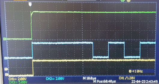
[22-APR-22] In LWDAQ 10.4.1 we add daq_wake_ms to the BCAM, Rasnik, Camera, and Thermometer instruments. We set daq_wake_ms to 0 and look at WAKE, !V2, and +15V on an A2075C. We are using an A2071E driver.

Figure: Wake-Up and Sensor Clear, Delay In Software. We have daq_wait_ms = 0. Yellow: the WAKE bit. Blue: the vertical phase control !V2, which oscillates during sensor clear. Green: +15V waking up.
The new code transmits a wake command then executes a sensor clear job. The delay between the two is roughly 50 μs. The power supply turn on and settles in one or two microseconds. When we set daq_wake_ms to 1 ms, we see a 3-4 ms variable delay between WAKE and the clear job beginning. This is the round-trip time over TCPIP that the code requires to confirm that the wake job has been executed.
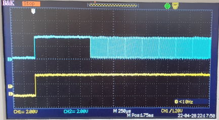
[29-APR-22] At CERN we find we see ambient light reflections when we set daq_wake_ms = 1, which we determine is due to the introduction of delays far greater than 1 ms when we acquire images from pairs of BCAMs. We improve daq_wake_ms implementation by running the delay on the driver. The delay is now 70 μs for daq_wait_ms = 0 and 1.25 ms when daq_wait_ms = 1. Thereafter the delay increases by exactly 1 ms per increment of daq_wait_ms.

Figure: Wake-Up and Sensor Clear, Delay In Hardware. We have daq_wait_ms = 1. Yellow: the WAKE bit. Blue: the vertical phase control !V2, which oscillates during sensor clear.
We apply this new implementation everywhere we have the wake-up delay and release with LWDAQ 10.4.2.


