 D-BCAM Head (A2086) Manual
©2017-2021, Kevan Hashemi, Brandeis University© 2021-2023, Kevan Hashemi, Open Source Instruments Inc.
The D-BCAM Head (A2086) is a Long-Wire Data Acquisition (LWDAQ) Device that reads out two ICX424 (or equivalent) image sensors and controls four light sources. The image sensors are mounted on two ICX424 Minimal Heads (A2076) connected to the A2086 board with two 12-way flex cables. The light sources are mounted on two Dual Laser Heads (A2074) connected to the A2086 board with two 6-way flex cables.

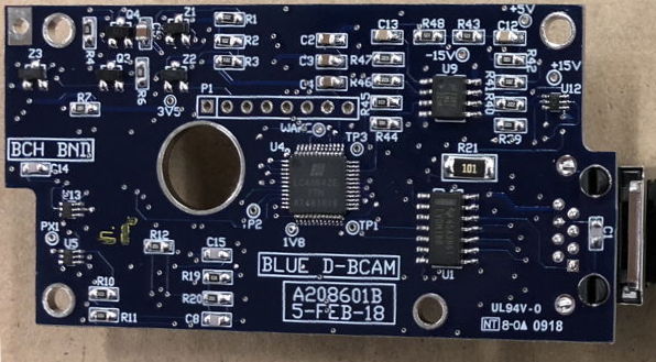
The D-BCAM Head is similar to the N-BCAM Head (A2083), but accommodates a second sensor with the help of pairs of the radiation-tolerant n-channel mosfet UM6K34N, and controls two more laser diodes with command bits DC12 and DC13. The assignation of LWDAQ element numbers for the two cameras and four lasers is identical to the Polar BCAMs.
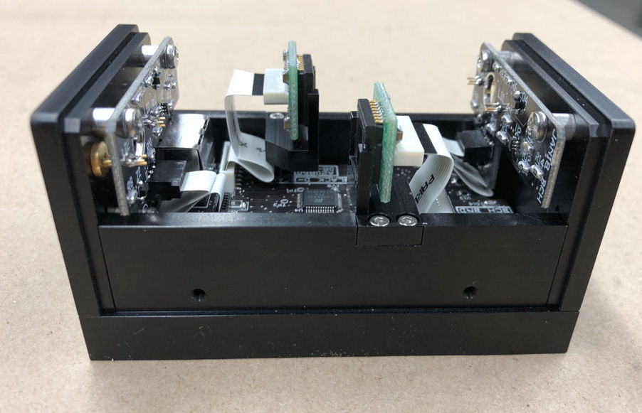
The Black and Blue D-BCAMs both use the same ICX424 Minimal Head, the A2076J. But the Laser Heads are different, because they must be mirror images of one another. The Black D-BCAM uses the A2074E and the Blue D-BCAM uses the A2074F.
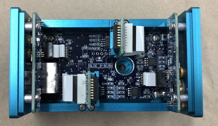
With the cover on, the D-BCAM has only two openings through which dust can penetrate to land upon its image sensor: the hole in the lid and the hole in the base that allow us to fasten the chassis to its kinematic mount with an M4 screw.

We cover these two holes with electrical tape before shipping the finished device. The serial number on the front face allows us to identify the BCAM in large systems where our database of location and serial numbers has been corrupted. The front number is the lower three digits of the main serial number.
Note: All our schematics and Gerber files are distributed under the GNU General Public License.
A208601_Drawing.gif: Dimensions of D-BCAM circuit board.[23-OCT-23] Circuits assembled on the A208601A/B/C printed circuit boards require C16, 10 nF loaded from U11-3 to U11-4, which provides decoupling of −15 V to 0V. This decoupling stops oscillations of the ±15 V power supply that arise on these layouts. Without C16, some A2086 assemblies develop 2 Vpp 100 MHz oscillations on the power supplies as soon as we wake the board up. These oscillations arise by interaction of the non-linear switching transistors, the current drawn by the op-amps, and the inductance of the power distribution tracks.
The A2086A is a LWDAQ device of type ICX424 (6) when we read it out one pixel at a time, and device type ICX424Q (7) when we read it out with quadruple pixels. When we flash one of its LED arrays, we can use device type ICX424 (6) or ICX424Q (7), because these have the same allocation of bits for flash jobs. The A2071E and A2037E LWDAQ Drivers support both device types, but you will need firmware version 6+ for the A2071E and 18+ for the A2037E. The A2086A does not implement the functions of the enhanced ICX424 and ICX424Q device types. The table below gives the device bit allocations implemented by the A2086A.
| DC16 | DC15 | DC14 | DC13 | DC12 | DC11 | DC10 | DC9 | DC8 | DC7 | DC6 | DC5 | DC4 | DC3 | DC2 | DC1 |
|---|---|---|---|---|---|---|---|---|---|---|---|---|---|---|---|
| PXBN | X | X | ON4 | ON3 | ON2 | ON1 | CCD1 | WAKE | LB | SUB | V3 | V2 | V1 | H | RDP |
The PXBN bit enables pixel binning to produce quadruple-sized pixels. The V1-V3 bits control the three vertical phases of the IXC424. When we assert the CCD1 bit, we select image sensor No1. Otherwise we select sensor No2. When we assert ON1-ON4 we turn on sources No1 to No4. The table below gives the sixteen-bit commands we can send to the A2086 to turn on one or more of its light sources. As we turn on more than one, they must share the available current. When we calibrate lasers, we turn on only one laser at a time to make sure that we are driving the laser to full power.
| Command | Effect |
|---|---|
| 0x1080 | Turn on source number 4, maximum 150 mA. |
| 0x0880 | Turn on source number 3, maximum 150 mA. |
| 0x0480 | Turn on source number 2, maximum 150 mA. |
| 0x0280 | Turn on source number 1, maximum 150 mA. |
| 0x1880 | Turn on sources 3 and 4, maximum 75 mA each. |
| 0x0680 | Turn on source 1 and 2, maximum 75 mA each. |
| 0x1E80 | Turn on all sources, maximum 37 mA each. |
The A2086A does not use DC14 and DC15, which give the Virtual Device Type in the enhanced ICX424 device behavior. All four virtual devices supported by the enhanced behavior are handled the same way, as a dual image sensor, quad light source device with optional quadruple-pixel readout. When we are capturing an image of the BCAM's own lasers, we must specify that the LWDAQ operate with source device type IXC424 (6) or ICX424Q (7) as well as camera device type IXC424 (6) or ICX424Q (7). When accumulating an image in the ICX424, we must hold vertical clock phase V1 low. If we flash one of the A2086 lasers using another device type, V1 will not be held low, and the White Rectangle Error appears, like this.
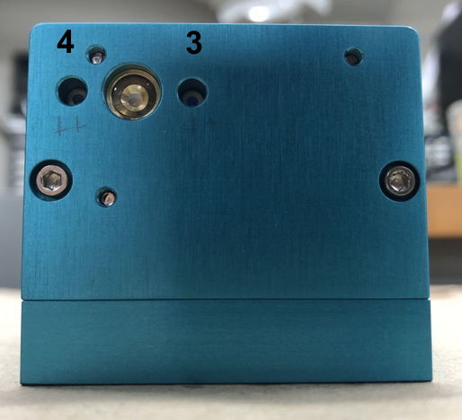
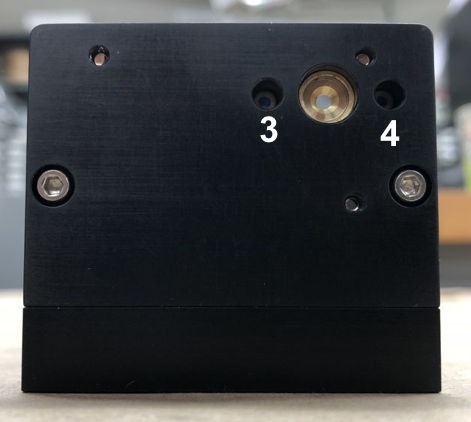
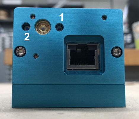
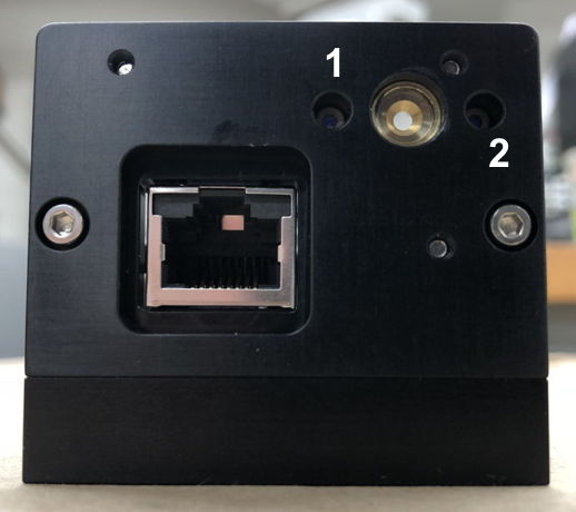
The front-facing lasers are element numbers 3 and 4, and work with the front-facing camera, which is element number 2. The rear-facing lasers are 1 and 2, and the rear-facing camera is 1.
The A2086 uses two pairs of UM6K34N mosfets as switches to select between the two image sensor outputs PX1 and PX2. According to our tests with x-rays, the threshold voltage of this 0.9-V mosfet drops by less than 0.1 V after 1.3 kGy. We used pairs of a similar mosfet, the UM6K31N, in the LWDAQ Multiplexer (A2085) to select from fourteen sets of LWDAQ return signals. In the A2085, the analog switches had to accommodate input voltages in the range −0.7-5.0 V. The threshold voltage of he mosfet had to be greater than 0.7 V to make sure we could disconnect a voltage of −0.7 V. The UM6K31N has a threshold voltage 1.0-2.3 V. In order to be sure to connect a voltage of +5 V with a threshold voltage of 2.3 V, we provided a 7.5 V voltage level for the gate drive of the mosfets. In the case of the A2086, the two pixel voltages are already AC-coupled onto VCOM = 1.4 V and have a maximum deviation of ±0.4 V. The UM6K34N threshold of 0.3-0.9 V permits us to connect 1.4±0.4 V with a gate voltage of 2.7 V or higher. Our logic power supply is nominally 3.5 V, and will be at least 3.1 V given +5V power is guaranteed to be 3.1 V or above, and the saturation voltage of Q2 is tens of millivolts. We can disconnect 1.4±0.4 V with a gate voltage of 0.1 V or lower. Our logic output is <100 mV for a high-impedance load like a mosfet gate. Thus we are able to make simple analog switches for our pixel voltages using pairs of these mosfets. We use the same mosfets to switch on the laser diodes. With a gate voltage of 3.5 V, the UM6K34N has typical channel resistance less than 1.7 Ω. This resistance is insignificant compared to the 100-Ω series resistor R21 we use to drop the +15V we provide to the two A2076 dual laser heads.
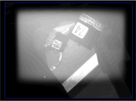
The D-BCAM is device type 6 (ICX424). If we use the same LWDAQ commands to flash its lasers as are used for device type 2 (TC255), the lasers will flash correctly. But if at the same time, the D-BCAM is acquiring an image, and we hope to illuminate the field of view with its own laser light, we will find that these TC255 commands disrupts the exposure of the D-BCAM's image sensor. In roughly half of D-BCAMs, we will see a white square in our image, as above. In the other half, we see no effect. Use device type 6 for daq_source_device_type in the Info Panel of the BCAM Instrument to obtain a reliable image.
he following table shows the quiescent current of several un-irradiated circuits with no sensors or sources attached.

We add the following current consumption entries to the Analyzer Tool database.

Waking up the board turns on all the ±15V power supply. The power supply switch consumes 7 mA from +15V and 3 mA from −15. The op-amps consume tens of milliamps together. When we add two image sensors (CCDs), they consume another 13 mA from +15V only.
[06-SEP-23] See Image Dynamic Range in Bar Head (A2082) manual.
[06-SEP-23] All the components uses on the A2083 are also used in the same way on the A2082. We discuss the radiation tolerance of these components in the Bar Head Manual.
[05-FEB-18] The A208601A printed circuit board is fully functional after correcting two errors on the schematic. First, R+ and R− were switched around on the outputs of the video amplifier outputs. Second, we must connect A to B with a wire because there is no spare logic gate in U4 to provide the connection.
[09-FEB-18] We correct A208601A and submit for fabrication as A208601C.
[15-FEB-18] We have completed the A208601B layout for the Blue D-BCAM main board and submit for fabrication.
[26-FEB-18] Firmware P2086A03 changes the pin used for signal A to match the updated Black N-BCAM layout, the black-masked A208601C, which we received last week. The circuit board now functions correctly. We measure the delay between the rising edges of A, DA, and DDA, which should be 125±25 ns.


[01-MAR-18] We prepare P2086A03.jed compiled so as to provide power-up reset for all registers, slow slew rate on all outputs, and defined 3.3-V logic levels on all outputs, and holding rather than pull-up or pull down. Our hope is that the power-up state of these ZE logic chips, when programmed in this way, will be reliable.
[26-APR-18] We find that the saturation brightness of D-BCAM images is less than the 255 counts we are used to from N-BCAMs. We expose an image sensor to overhead lights and observe PX2 falling with a time constant of around 100 ns, while its rise time is much faster. We are using U6 to connect PX2 to U7-5. When we select PX1 instead, the fall time on PX2 matches the rise time, as it does in the N-BCAM. We select PX2 again and remove U5, R17, and R18 in turn, still have slow fall time. The gates of both U6 mosfets are at 3.5 V. The sources and drains are following PX2. We replace U6 with a wire and now the fall time is fast.
We calibrate a prototype D-BCAM-L on our roll cage using our new octal source block, flashing the outer four sources only with a 36-Way Light Injector (A2080B). We use the following sketch deduced from the machine shop drawings.

We use the above dimensions with respect to the straight edge and table surface for our source positions in a prototype apparatus description. With a micrometer we determine that the tips of the ferrules in the large source block are 11.4 mm closer to the roll cage than the laser diodes in the old source block, so we subtract 11.4 mm from the ranges we used with the old source block. In the view of the D-BCAM, serial number E00001, the source block at the near range looks like this.
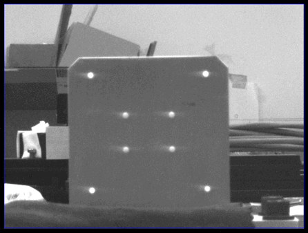
We calibrate ten times as a black H-BCAM and get the following calibration constants and standard deviations.

Our pivot-ccd and pivot.z stability appears to be a factor of three better than we obtained with the old source block.
[30-APR-18] When U6 is turned on, so as to connect PX2 to U7-5, the gate capacitance of its two mosfets are in parallel to 3.5 V and must be discharged when PX2 falls and charged when PX2 rises. According to the UM6K34N data sheet, its typical gate capacitance is 26 pF, so two together is 52 pF. We expose our image sensor to overhead light. We connect a resistor from PX2 to 0V and look at the voltage on U7-5.


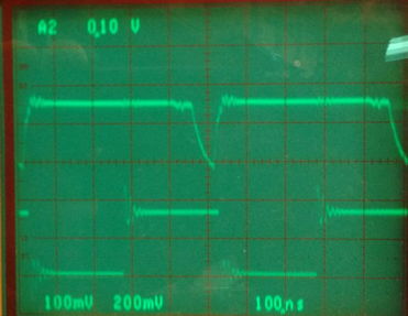
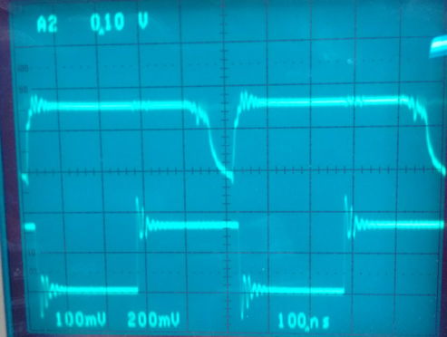
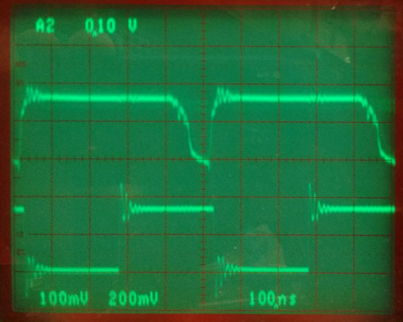
The fall-time decreases from approximately 150 ns to 40 ns as we go from no drain resistor to 900 Ω. The rise time remains roughly 10 ns. The output of the ICX424 is the drain of a mosfet buffer. It appears that the resistor in series with the drain is of order 3 kΩ. When combined with our 50-pF channel capacitance we get a time constant of around 150 ns.
We note that the pixel pulses are only 100 ns long, compared to 200 ns in the A2083 and A2082. Our P2086A04 firmware is in error. We correct the firmware and lengthen the pulses. Now we see the following with no added drain resistor. With the P2086A05 firmware, we get bright white images from saturated sensors.
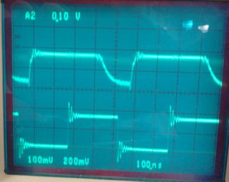
[02-MAY-18] We have CMM measurements of the new source block. We incorporate these into a new apparatus entry for both the front and rear Black D-BCAM cameras. We calibrate E00001 front and rear with the old source block (BND10 apparatus) and the new source block (BND11 apparatus).

[25-SEP-23] We are making 20 new A2086A by hand. We find that some of them show 2-Vpp 100 MHz oscillation on H1 and H2, and on ±15 V power supplies. We remove several op-amps and the oscillations stop. We load them again. We add 1 nF between the emitter and collector of both Q4 and Q5 to provide a high-frequency connection between the switched ±15V power supply and the decoupling capacitors on the raw ±15V power. The oscillations vanish. We add to C16 and C17 to the schematic.
[18-OCT-23] The C16 and C17 modification does not always stop oscillations. We find that it is the inductance of the ±15V power traces on the circuit board that cause our decoupling to be ineffective. We remove C16 and C17 from the schematic and resolve to correct the layout of both black and blue D-BCAM base boards so as to stabilise the power supplies. The instability does not, however, have any effect upon the performance of a completed BCAM. To stop oscillations more easily, we load 10 nF from U11-5 to U11-4, which decouples −15V to 0V, and this seems to be sufficient.
[23-OCT-23] We eliminate the Two-Capacitor Modification in favor of one C16=10nF from −15V to 0V, which we load from U11-3 to U11-4. This addition stops oscillations on all boards.