 Fourteen-Way Multiplexer (A2085) Manual
©2015-2021, Kevan Hashemi, Brandeis University© 2021-2022, Kevan Hashemi, Open Source Instruments Inc
The Fourteen-Way Multiplexer (A2085) is a LWDAQ Multiplexer in a metal enclosure that provides fourteen branch sockets. Its shielded root socket connects to a LWDAQ Driver (such as A2071 or A2037) with a LWDAQ root cable. Its fourteen un-shielded branch sockets connect to fourteen LWDAQ Devices. Power is always delivered to all fourteen branch sockets (±15 V, 0 V, and +5 V). The LWDAQ transmit and receive signals, T+/T− and R+/R−, are connected to a subset of the fourteen branch sockets.
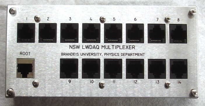
Any branch socket that passes transmit and receive signals is active. In normal use, only one socket is active. When the multiplexer is idle, no sockets will be active.

The enclosure has the same exterior dimensions as the Ten-Way Multiplexer (A2046A).
| Assembly Version |
Description | Firmware Version |
|---|---|---|
| X | Prototype, A208501A PCB, VS = 6.0 V | 1 |
| A | Production, A208501B PCB, VS = 7.5 V | 4 |
We made two A2085X circuits. We irradiated one in neutrons and the other in photons. Their connector rows were too closely spaced for the enclosure. The A2085A has the correct spacing for its enclosure. We had 150 of these assembled for us and loaded them into enclosures for the nSW upgrade to the ATLAS detector.
[23-DEC-15] The A2085 is a LWDAQ Multiplexer. It responds to LWDAQ Address Words, but ignores LWDAQ Command Words.
| DA15 | DA14 | DA13 | DA12 | DA11 | DA10 | DA9 | DA8 | DA7 | DA6 | DA5 | DA4 | DA3 | DA2 | DA1 | DA0 |
|---|---|---|---|---|---|---|---|---|---|---|---|---|---|---|---|
| X | 14 | 13 | 12 | 11 | 10 | 9 | 8 | 7 | 6 | 5 | 4 | 3 | 2 | 1 | X |
Activation of branch sockets is controlled by the A2085's sixteen-bit address word. These bits are DA0..DA14. Bits DA1..DA14 activate branch sockets 1 through 14. Bit DA0 is reserved for cooperation with a LWDAQ Repeater upstream or downstream of the multiplexer. Bit DA15 selects a local multiplexer loop-back virtual socket for diagnostic purposes. The address word is received via the T+/T− lines from the LWDAQ Driver. But it may be reset by the multiplexer logic, after the multiplexer has been idle for a some time. When all bits are zero, no socket is active, all mosfet switches are off, and all LVDS drivers are off.
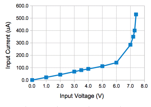
The R+/R− return signal is low-voltage differential, but can be analog or digital. When we select a branch socket, the A2085 analog switches connect R+/R− to the driver, where they are terminated by 100 Ω. The analog switches must pass all possible voltages on R+/R− when the signal is terminated. When R+/R− is a digital signal generated by an LVDS driver on the device, its common-mode voltage is 1.2±0.1 V and differential voltage is ±0.5 V for an LVDS multi-point driver with a load of only 100 Ω. When R+/R− is analog, the return signals are generated by op-amps. In most cases, the common-mode analog voltage is 1.4±0.1 V with a differential voltage up to ±0.5 V. But in some cases, such as the A2065, the device produces a pseudo-differential signal by setting one of the return lines to a constant voltage 1.4±0.1 V and varying the other in the range 1.4±0.5 V. When a device does not drive the R+/R− lines, the lines can either be in a high-impedance state, drawing no more than 1 μA, as for digital-only devices like the A2045, or they can be connected to 1.6±0.4 V through a few hundred ohms, as in analog-digital devices like the A2083.
All the voltage ranges specified in the previous paragraph were for R+/R− terminated with 100 Ω. But the A2085 does not provide terminating resistors for R+/R−. When a branch socket is not selected, its R+/R− will not be terminated. The voltage on these two signals can now lie anywhere in the clamping range specified for LWDAQ receive signals, which is −0.7 to 5.0 V. Thus the analog switches must provide isolation R+/R− lying within this range.
In summary, the voltage on the return signal will lie within the range 0.8-2.0 V when the switches are turned on, and −0.7-5.0 V when the switches are off.
The R+/R− signals on the multiplexer's root socket are connected to the active branch socket. If there is no active socket, they are held down to 0 V each by their own 100 kΩ resistor. To select which branch socket R+/R− signal is connected to the root socket, the multiplexer uses thirty analog switches each made out of a pair of n-channel mosfets. There are two switches for each of the branch sockets 1-14, and two for the virtual branch socket number 15. The sources of each pair of mosfets are connected together. The drain of one is connected to the device, and the drain of the other to the root socket. Their gates are connected together also, and pulled down to 0 V by 10 kΩ. We turn off the n-channel mosfets by allowing their gates to settle to 0 V. The unterminated R+/R− signals from the device will be at −0.7 V or higher. If the threshold voltage of the mosfets is 0.7 V or less, both mosfets will turn on when their drains and sources are at −0.7 V. The dual mosfets will provide isolation for R+/R− = −0.7 V only if their threshold voltage is greater than 0.7 V.
When we turn on the switches, the R+/R− signals are terminated at the driver, and now lie in the much smaller range 0.8-2.0 V. To switch on a pair of mosfets, we pull their gates up to VS. If we use the 5-V power supply for VS, we note that the LWDAQ specification allows +5V to drop to 3.1 V. In order to connect +2.0 V to the driver, we need a mosfet with threshold voltage less than 1.1 V. The UM6K34N provides a threshold in the range 0.3-0.9 V, with channel resistance no more than 9 Ω and channel capacitance 26 pF. Because its threshold can be <0.7 V, however, this mosfet may be unable to provide isolation when R+/R− are at −0.7 V.
If we choose VS = +15 V, we will be sure to turn on our mosfets, but turn-off will be slower because we must discharge the mosfet gate capacitance all the way from +15V down to 0 V. The A2085 provides a 7.5-V voltage derived from +15V that we connect to VS. With VS = 7.5V, we provide a minimum of 5.5 V gate-source voltage. We can use the UM6K31N with threshold voltage at 1.0-2.3 V. With gate-source voltage 4.5 V the channel resistance is only 2.1 Ω and channel capacitance is 15 pF. Our ionizing irradiation of the UM6K31N shows less than a 0.3-V drop in threshold voltage after 1.3 kGy, so the threshold voltage will be >0.7 V even after 1.3 kGy. Ideally, we would like device loop-back to work even if the only device power supply available was +5 V. The disadvantage of deriving VS from +15 V is that when ±15 V fails, the multiplexer will no longer connect device loop-back to the driver, because VS will be absent.
We use two mosfet switches together for each branch socket, so we connect the gates of the four mosfets together and they share the same 10 kΩ pull-down resistor we can share the same PNP transistor to drive the gates when we turn on the mosfets. The turn-on will be fast, because the PNP transistor charges the four gate capacitances (4 × 15 pF = 60 pF) in a few nanoseconds. But the turn-off will take longer, as the 10 kΩ discharges the gate capacitances from +7.5 V down to 0.1 V in roughly 3 time constants, or 2 μs.
The transmit lines from the LWDAQ Driver, T+/T−, must be sent to some subset of the fourteen branch sockets. We would like the multiplexer to support transmission of commands to all branch sockets, although this is not required by the LWDAQ specification. Each branch socket, and the virtual branch socket that provides local loop-back, is equipped with its own LVDS driver. The SN65LVDS1 comes in an SOT-23-5 package, and is in the same family as the SN65LVDM180D, which we have used for fifteen years, and whose radiation tolerance we know well. The SN65LVDS1 does not have an enable line. But its inputs and outputs are high-impedance when VCC is less than 1.5 V. Thus we can enable and disable each driver by turning on and off its power supply. We deliver power to the drivers with the branch socket select lines TX1-TX15, where TX15 selects the virtual socket's driver. We provide a 1.0 nF decoupling capacitor on each of these lines so as to stabilize the driver. The same line is used to close the analog switches on R+/R−.
When an LVDS driver is disabled, we want the state of the outgoing T+/T− signal to be HI. In the LWDAQ Driver, T+ is pulled up to +5V by 10 kΩ, and T− is pulled down to 0V by 10 kΩ. We provide the same pull-up and pull-down resistors for each branch socket. But we use the 3.5 V power supply for the pull-up resistor rather than the +5V supply. We do not want T+ floating to +5V when the driver is disabled. According to the SN65LVDS1 data sheet, we should apply no more than 4 V to this output. On the LWDAQ Driver, a disabled T+ signal is isolated from its LVDS driver by an analog switch, and we want the pull-up voltage to be one that is switched on and off along with the device power, so we did not use the local 3.3-V logic supply. We used the +5-V device power, which turns off when we turn off power to the devices. On the A2085, the 3.5-V supply is on only when the incoming +5-V device power is on, so we can 3.5 V for our pull-up without any risk of pulling up T+ for a device that has no power.
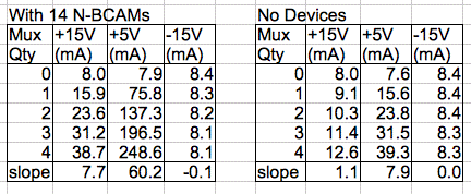
With no devices connected, the A2085A draws quiescent current 7.7 mA from +5 V, 1.1 mA from +15 V, and 0.0 mA from −15 V. When one of the branch sockets is enabled, an additional 2.5 mA will be drawn by the enabled LVDS driver, even if there is no device connected. If there is a device connected to the enabled socket, the enabled LVDS driver will consume a total of 4.5 mA. When we have fourteen N-BCAMs attached to the multiplexer, the total current drawn by the multiplexer and devices when all the devices are asleep and all branch sockets are disabled is 60 mA from +5 V, 7.7 mA from +15 V, and 0.0 mA from -15V. When we turn on LWDAQ Power, the A2085 firmware usually start up with all socket enable lines TX1-15 unasserted. But with an 80-m root cable, half the time we will find that one of the enable lines is asserted. The P2085A firmware, versions 2+, ensure that no more than one enable line can be asserted at a time. For more details see below.
[04-JAN-15] Schematic is complete. Our design uses the SN65LVDS1 line driver. The part has no disable input and its quiescent current with driver enabled is typically 5.5 mA with a 100 Ω terinating resistor at the device. If these drivers were left enabled at all times, we would have typical quiescent current of 77 mA with 14 devices connected, and maximum 112 mA. We disable individual drivers with the lines TX1..TX14, which act as power to the driver as well as select for the mosfet switches. The equivalent circuit for the SN65LVDS1 input is a 7-V zener diode and 300-kΩ resistor to 0 V. We take out an SN65LVDS1 and connect VCC and GND to 0 V. We connect the D input to a voltage, V, and measure the current flowing into D with an ammeter.
The input current for an applied 3.5-V logic level is 80 μA. Fourteen such disabled drivers will draw 1.1 mA, which is much less than the 20 mA allowance from +5V for a multiplexer.
[07-APR-16] Our A208501A printed circuit board was functional, but the connector rows were too close together for our enclosure. We built two of the A2085A. One we irradiated to 1.4 kGy and the other we sent for a neutron test. At 1.4 kGy the A2085A remains fully-functional. We move the two rows of connectors 2 mm out towards the edges of the board in the A208501B. We have three of the A2085B with A208501B printed circuit board. They work well. They use the UM6K31N mosfet. We note that VS is 6.0 V instead of 7.5 V, because R79 = 1.0 kΩ, which drops 1.5 V with the current drawn by an enabled mosfet switch. We change R79 to 0.0 Ω. The threshold voltage of the mosfets must be greater than 0.7 V, not 0.0 V, so the raditaion-resistant UM6K34N is not going to work in the A2085 when any R+/R− line is clamped to −0.7 V.
[28-APR-16] We subject an A2085X to 15 Tn of fast neutrons at the UMass Lowell reactor. Afterward, its connectors are active and we leave it in a draw for a few days. We capture images from all branch sockets. The multiplexer behaves normally.
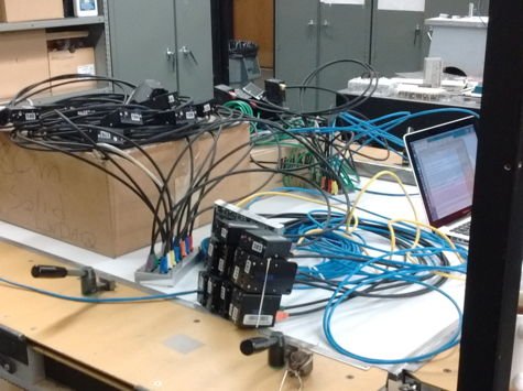
[20-MAR-17] We have a test stand set up, consisting of one LWDAQ Driver (A2071E), three A2085A and a total of 36 Black N-BCAMs. Every couple of minutes we turn on LWDAQ power and capture images from all multiplexer sockets before turning off the LWDAQ power. We use our Test_Stand.tcl Acquisifier script.
The script has been running continuously for five days. Each execution records the loop time of all multiplexer channels. These have remained the same. This is our burn-in test of the multiplexers, after which we are willing to ship them to Europe.
We stop the Acquisifier script and turn on the LWDAQ power. One of the BCAMs has both lasers shining continuously. It is connected to the 80 m root cable. We investigate the power-up current consumption as follows.
| Action | +15V (mA) | +5V (mA) | −15V (mA) |
|---|---|---|---|
| On | 143.215 | 216.796 | 42.680 |
| Sleep All | 32.583 | 180.561 | 8.153 |
| Disconnect 20 m root cable (socket 6) | 25.256 | 128.256 | 8.194 |
| Disconnect 40 m root cable (socket 7) | 16.094 | 62.015 | 8.294 |
| Disconnect 80 m root cable (socket 8) | 7.994 | 8.028 | 8.391 |
| Reconnect 80 m root cable (socket 8) | 18.824 | 68.169 | 8.311 |
| Reconnect 40 m root cable (socket 7) | 26.587 | 129.979 | 8.214 |
| Reconnect 20 m root cable (socket 6) | 33.910 | 184.157 | 8.164 |
| Off-On | 162.966 | 176.392 | 68.838 |
| Off-On | 44.998 | 211.945 | 8.153 |
| Transmit Address 1E | 45.085 | 212.091 | 8.105 |
| Transmit Address 6E | 46.564 | 214.829 | 8.051 |
| Transmit Address 7E | 46.497 | 214.745 | 8.123 |
| Transmit Address 8E | 31.166 | 176.296 | 8.170 |
| Sleep All | 32.517 | 180.531 | 8.220 |
| Off-On | 49.358 | 223.234 | 8.057 |
| Off-On | 47.961 | 219.616 | 8.079 |
| Transmit Command 0x000 | 47.941 | 219.601 | 8.125 |
| Transmit Address 8E | 29.765 | 173.675 | 8.203 |
| Off-On | 63.296 | 271.696 | 8.022 |
Following the last action, we check signals TX1-15 on the socket-8 multiplexer (80-m cable) and find all 15 are asserted. All fifteen LVDM drivers are enabled. On the socket-7 multiplexer (40-m cable), 9 of 15 are asserted. On the socket-6 multiplexer (20-m cable) 0 of 15 are asserted.
| Action | +15V (mA) | +5V (mA) | −15V (mA) |
|---|---|---|---|
| Sleep All | 32.571 | 180.479 | 8.155 |
| Transmit Address 80 | 31.142 | 176.689 | 8.203 |
After a Sleep-All, the device address is 8F, and the dummy socket on the multiplexer is enabled. We transmit 80 and now no multiplexer socket is enabled. Current consumption drops by 3.8 mA on +5 V. According to the SN65LVDS1 data sheet, the current consumption of one enabled LVDS driver is typically 5.5 mA. With 24 LVDM drivers enabled rather than only one, we expect an 87-mA current increase. We observe 272-174 = 98 mA. Looking at the P2085A01 firmware, the TX1-15 signals are equal to DA0-15, the device address signals. These are not powering up zero every time when on the end of a 40-m or 80-m cable.
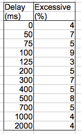
[22-MAR-17] We have new firmware P2085A02, in which each TXn signal is asserted only if DAn is asserted and all other DA bits are un-asserted. The variation in +5V current consumption after power-up for the three multiplexers is now 169-181 mA, which suggests that we have between zero and three LVDS drivers enabled after reset. We note that the BCAM connected to driver socket 8, multiplexer socket 1 sometimes powers up with one or two lasers on, and their current consumption is apparent in +15V. No other socket produces this problem, and the problem occurs with any cable and any BCAM on this socket. With an oscilloscope probe on the TX1 line, we see pulses on power-up. But now we see other BCAMs on socke 8 turning on at power-up as well. We set up the Diagnostic instrument to turn off the power, wait for m milliseconds, turn on and measure current consumption. We try this for various values of m.
We add another multiplexer with fourteen BCAMs and six more BCAMs to the existing multiplexers. We cycle power off, wait 500 ms, turn on, and measure current consumption. Out of 100 trials current consumption on +15V is 38-41 mA, −15V is 8.2-8.4 mA, and +5V is 244-254 mA.
[23-MAR-17] We have four multiplexers each with fourteen N-BCAMs connected. We measure current consumption as we plug then into our LWDAQ Driver so as to obtain a measurement of sleep current versus number of fully-loaded multiplexers.
We connect another multiplexer with two BCAMs and run all five multiplexers and 54 BCAMs in the test stand.
[29-MAR-17] We have been running 5 multiplexers and 54 BCAMs for 144 hours, powering up every ten minutes. On 124% of the power-ups, between one and three BCAMs are awake. The +5V current after power-up varies from 257-276 mA. We see no changes in loop times for any cable.
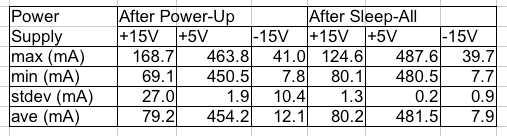
[06-APR-17] After ten days running with 5 multiplexers and 54 BCAMs the +5V current after power-up has range 47-228 mA, +15V is 285-309 mA, and −15V is 8-75 mA. We expand the system to 8 multiplexers and 112 BCAMs. After power-up we measure current consumption, execute a sleep-all, and measure current consumption again. Our acquisifier script contains 248 steps, see Test_Stand.tcl. We arrange the BCAMs so that, with overhead lights illuminated, we obtain ambient light images from all of them. We run ten times and +5V current range is 452±1 mA, +15V is 70±1 mA, −15 is 80±1 mA. We leave running every ten minutes.
[12-APR-17] After fifteen hundred cycles of power, sleep-all and image capture from all 112 BCAMs, the power supply current consumptions after power-up and after sleep-all have the following ranges.

On one occasion, the ±15V current consumption remained high after the sleep-all: 180 mA and 41 mA from +15V and −15V respectively. Following the sleep-all, the loop times of all 112 BCAMs are correct.
We note that the metallic enclosure of our A2085A is close to the 0V test pads on two corners. Contact between 0V and the chassis would violate the LWDAQ grounding rules. We check for contact between 0V and the chassis on twenty multiplexers in their chassis, and find no contact in any of them.

We do, however, discover the following assembly error. As a result of this assembly error, the circuit board is bent in one corner. We repair the assembly. There was no contact between chassis and 0V before or after the repair. We swap out all eight multiplexers of our test stand.

New multiplexer 20MNABNDM00135 produces bad images on socket 12, which we trace to a faulty TX9 LVDS driver. The images contain horizontal streaks. After repair, we note bad images on socket 9 in the test stand, but not at our work bench. In the former case we have a 120-m cable and in the latter a 6-m cable. But the oscilloscope reveals that the LVDS voltages levels are wrong. The T+ drive appears to be weak or absent. We replace the LVDS driver and all is well. We conclude that we must test all multiplexers with a long root cable, or check all T+/T− levels with the oscilloscope.
[24-APR-17] After 3500 cycles, there are 450 cycles in which the +15V current is >90 mA after power up and 8 cycles in which the +15V current is greater than 90 mA after the sleep-all. Whenever the current is high after sleep-all, it is within ±10 mA of the current after power-up.
[04-MAY-17] We have gone through our entire stock of A2085As and found two with the assembly error, which we corrected. Another set of multiplexers tested for eight days, ranges below.
[11-MAY-17] We load another eight multiplexers into our test stand. One has two bad channels with damaged LVDS drivers. Both channels capture images with a 5-m cable, but not with an 80-m cable. We replace the drivers and the transistor in the VS circuit. We add 20 m of root cable to the two root cables less than 40 m, so that all are 40 m or greater. All 112 BCAMs capture images and loop back correctly.