 Contact Injector (A2080) Manual
©2014-2021, Kevan Hashemi, Brandeis University©2021-2024, Kevan Hashemi, Open Source Instruments Inc.
| 2014 | 2015 | 2016 | 2017 | |
| 2018 | 2019 | 2021 | 2022 | |
| 2023 | 2024 |
The Contact Injector (A2080) is LWDAQ device of type multisource (9) that provides one or more light emitting diodes (LEDs) for injecting light into optical fibers without the use of a lens. The A2080 circuit is designed to drive any type of LED. It provides a drive voltage of up to 4.2 V and drive current up to 1.0 A. The A2080B, for example, provides 36 separate, individually-fused buck converters to power 36 deep-red Luxeon-Z LEDs. Only one LED can be driven at full power at a time, but by flashing one LED after another for a brief time, the circuit can provide the illusion of all LEDs being illuminated dimly at the same time.
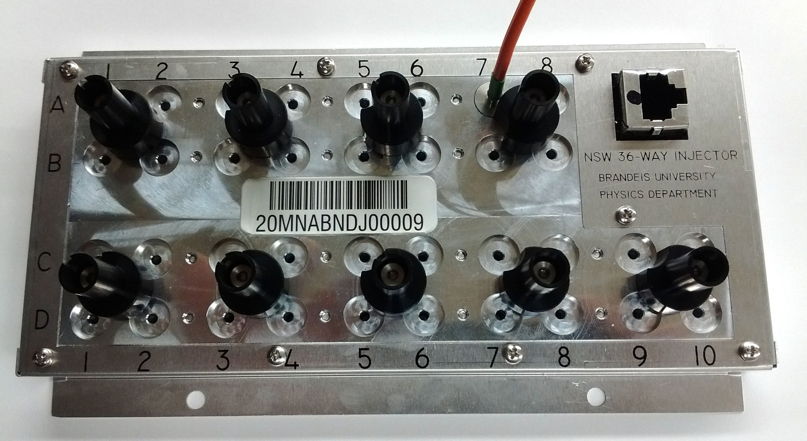
The fully-assembled A2080B is equipped with a face plate to hold the optical fibers and an enclosure for protection. We push a 2.5-mm diameter ferrule into any one of the holes in the face plate and hold it in place with a locking knob to ensure repeatable contact injection. The face plate serves also as a heat sink for the LEDs, which dissipate up to 2 W with 1000 mA passing through them.
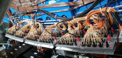
The A2080 uses buck converters to transform the LWDAQ ±15 V power supply into an LED drive power supply. The LED drive voltage is equal to the forward voltage drop of the selected LED plus a small voltage across a 0.1-Ω current sensing resistor. Blue and white LEDs have a forward voltage drop of around 3.2 V. At a forward current of 1000 mA, the drive voltage will be around 3.3 V.

The A2080A and A2080B are equipped with Luxeon-Z LEDs. The A2080B is loaded only with Luxeon-Z LXZ1-PA01 deep-red LEDs, and provides a maximum LED current of 800 mA when there is no magnetic field present, and 1000 mA in a 500-mT field. The forward voltage of these LEDs is around 2.1 V. When the buck converter provides 800 mA to an LED, it draws 85 mA from the ±15 V power supplies.
| Version | Description |
|---|---|
| 2080X | 36-Way Injector with Various Luxeon-Z LEDs, green A208001D PCB. |
| 2080A | 36-Way Injector with Deep-Red Luxeon-Z LEDs, blue A208001E PCB. |
| 2080B | 36-Way Injector with Deep-Red Luxeon-Z LEDs, red A208001F PCB. |
The A2080B is designed for use in the New Small Wheel of the ATLAS detector at CERN. The circuit and its buck converters will continue to operate after 1 kGy of ionizing radiation, 10×1012 1-Mev eq. n/cm2 neutron radiation, and in the presence of a 0.5-Tesla magnetic field. You will find our study of the performance of inductors in strong magnetic fields here. The contact injection takes place with zirconia ferrule, which presents the polished end of an optical fiber to the 1-mm square LED at a range of 0.2-0.7 mm.
[26-AUG-24] The P2080A03 firmware provides power levels zero to ten and single-LED control. We turn on LED number n to power level p by sending command n8p, where n is a two-digit hex value specifying the LED and p is the power level. The lowest element number is 1 and the highest is 58, but not all the values 1-58 are used. The A2080B maps element numbers to alpha-numeric grid numbers according to the multisource device rules.
| Command (Hex) |
LED Number | LED Code | Power Level |
|---|---|---|---|
| 0000 | 0 | None | Off |
| 0080 | 0 | None | Off |
| 0101 | 1 | A1 | Low |
| 0107 | 1 | A1 | 7 |
| 0187 | 1 | A1 | 7 |
| 0886 | 8 | A8 | 6 |
| 2487 | 36 | C4 | 7 |
| 3A84 | 58 | D10 | 4 |
| 1985 | 25 | None | Off |
The Flash_All Toolmaker script will use the Diagnostic Instrument to flash all the LEDS on an injector one after the other using commands like those above. To use the Contact Injector with the BCAM or Rasnik Instruments, specify daq_source_device_type = 9 (multisource device) and make sure your LWDAQ Driver is equipped with firmware that can control such devices. No version of the LWDAQ Driver (A2037A/E) can flash a multisource device. A LWDAQ Driver (A2071A/E) must have firmware version 9+ to flash multisource devices. For the daq_source_element_num enter the LED number as defined in the diagram below, or the alpha-numeric grid number as defined by the chassis.
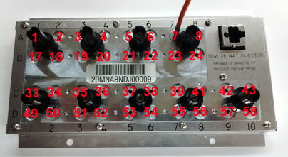
The A2080B is marked with rows A-D and ten columns 1-10. When connecting fibers to LEDs in the ATLAS experiment, we expect to be referring to LEDs by theiry alphanumeric grid coordinate A1 to D10. The Rasnik and BCAM Instruments of LWDAQ 8.5.21+ accept these grid coordinates for multisource devices, as well as the actual element numbers. In LWDAQ, we convert alpha-numeric codes into source element numbers with the LWDAQ_set_multisource_element.

The buck converter circuit works by connecting 30 V to an inductor for a few hundred nanoseconds, charging up the inductor's magnetic field, and then allowing the magnetic field to drive current through the LED for a few microseconds. Transistor Q1 turns on and off transistor Q2, which connects and disconnects 30 V. When the inductor is not connected to 30 V, it is discharging through diode D1.
[06-AUG-18] We take thirty A2080Bs with face plates and measure power injected into the same optical fiber jumper from each of their 1080 LEDs. We turn each LED on to full power (800 mA, power level 7, firmware version 6). We measure the power coming out of the other end of the fiber. The fiber is S705T-02F-62N3, 62-μm core, 125-μm cladding, NA=0.275 radiation-tolerant fiber with a 2.5-mm diamater zirconia ferrule.
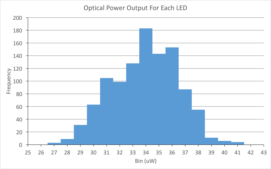
Average power 35 μW. If we assume a Lambertian radiation pattern from the LED, in which the LED emits light uniformly in all directions above its surface, we can estimate the fraction of light incident upon the fiber that will be captured by its core.
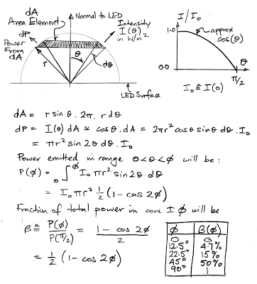
Our fiber has numerical aperture 0.275, meaning it captures light in a ±16° cone. Of the incident Lambertian light, our calculation suggests that our fiber will capture only 7.6%. If we assume uniform distribution of power over the 1-mm square surface, our 62-μm core will be illuminated by 0.3% of the total emitted light. We expect 0.02% of the LED's light to be capture in the fiber core. According to our measurements, the deep-red LED emits 240 mW at 800 mA (power level 7), so we expect to see 55 μW of power injected into our fibers if their radiation pattern is Lambertian. It turns out that their radiation pattern is less favorable for us than the Lambertian cosine pattern, as we present here. As a result, we capture roughly half the light our Lambertian calculation suggests.
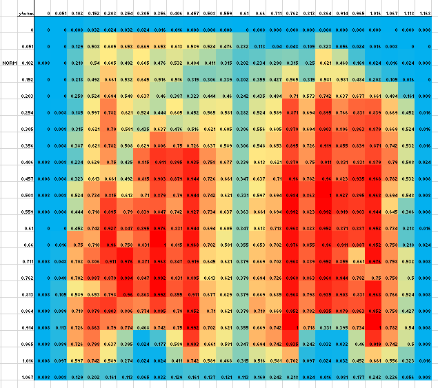
[13-JUL-17] The distribution of light across the 1-mm square emitting surface of a typical LXZ1-PA01 deep-red LED is shown below.
When we move the same 62-μ diameter fiber back 1 mm from the emitting surface of the same LED, we obtain the following map. Fluctuations in intensity are smoothed out by the mixing of light from various parts of the LED on its way to the fiber tip.
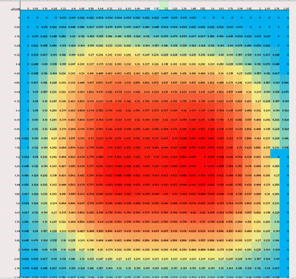
A 62-μm diameter fiber with numerical aperture 0.28 placed 1-mm above a deep-red Luxeon-Z LED carrying 900 mA will capture 40-50 μm of red light. We present a series of measurements of contact efficiency between fibers and LEDs in Contact Efficiency. With a microscope we measure the location of the center of the LED package with respect to the center of its footprint, and obtain the following scatter plot for the thirty-six LEDs on one factory-made injector.
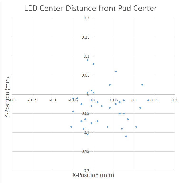
The average position is (+25 μm, −31 μm) where x is in the direction of the long side of the injector board. The maximum distance from centered is 135 μm in X and 105 μm in y.
[31-MAY-18] We load all eight colors of Luxeon Z chip-scale LEDs onto A1-A8 in an A2080A. In A1 we have the Royal Blue 450 to Deep Red 655 nm. We turn on each LED to power level seven (7) and measure the power out the other end of a 2-m 62-μm core, NA=0.275 optical fiber .

The efficiency of the LEDs in converting electrical power into optical power varies greatly with wavelength, the 470-nm LED being the most efficient, and the 590-nm LED being the least. The electrical power delivered is only a weak function of wavelength. The forward voltage drop of the 470-nm LED is 3.15 V, and of the 655-nm LED is 1.75 V. But the A2080A buck converter delivers electrical power in proportion to the duty cycle of its switching signal, and this duty cycle is the same for all eight LEDs. The variation in the above measurements is dominated by the relative efficiency of the LEDs.
[24-MAY-18] With 1000 mA flowing through an LXZ1-PA01 deep-red LED, we expect a forward voltage of around 2.0 V, so 2 W will be dissipated by the LED package. The A2080B circuit board is designed to transport this heat efficiently from the LED to nearby points of contact with the injector face plate.

The A2080B LEDs are arranged in sets of four. There are nine sets of four on one A2080A/B printed circuit board. In the photograph above we see the wide copper planes around the LED packages, and the four contact points marked on the silk screen. At each contact point, the circuit board is screwed to the aluminum face plate.
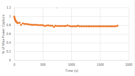
When we turn the LED on to full power, it takes roughly one minute to reach thermal equilibrium with the circuit board, face plate, and ferrule. The ferrule is a few hundred microns away form the LED package, but it stops almost all the light emitted by the LED from propagating away from the LED package. After one minute, the optical power emitted by the LED has dropped by 20%. For more details of heating and output power see Heat Effects.
The A2080A is designed for use in the New Small Wheel (nSW) upgrade of the ATLAS detector at CERN. Its planned installation location will be roughly 6.8 m from the interaction point along the beam line, at a radius of 4.0 m. The nSW itself is located at radius 7.0-7.9 m, on the far side of the iron shielding disk called JD.
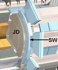
According to our radiation maps and estimates, the ionizing and neutron doses at the A2080A installed location will be slightly lower than in the nSW at the same radius. We use the nSW dose at radius 4.0 m as our guide, for which we have 30 Gy and 3 Tn after 3000 1/fb integrated luminosity.
[04-MAY-17] We test our prototype A2080A in ionizing radiation starting today, see here. All silicon components of the A2080A have already been tested in both ionizing and neutron radiation with the exception of the ZLLS2000 Schottky diode of the buck converter. The NDS355AN gate threshold voltage drops by roughly 1.2 V after 2 kGy. We use the NDS355AN for the switches on the logic level switch in the buck converters, Qn1. Assuming an initial gate threshold voltage of 1.6 V, which is what we have observed of our NDS355ANs and is the typical value specified in the data sheet, the logic level switch will still be effective at 2 kGy. The NDS356AP gate threshold drops by roughly 0.9 V after 2 kGy. We use the NDS356AP for the main buck converter switch, Qn2, where we apply a gate-source voltage of 0V and −5V as determined by resistor divider Rn3 and Rn2. The mosfet should continue to operate well past 2 kGy. Both mosfets are unaffected by neutron radiation up to 22 Tn. The deep red LED is the one we plan to use in the nSW, part number LXZ1-PA01. This LED loses 75% of its output power after 14 Tn of neutrons, but our image acquisition can tolerate such a loss. The LEDs are unaffecte by 1.4 kGy of ionizing radiation. The logic chip and LVDM transceiver tolerate at least 1.4 kGy as well, and 16 Tn.
[15-MAY-17] Two deep-red, one green, and one white Luxeon-Z LEDs have endured 550 Gy, while their buck converter circuits have endured roughly 500 Gy, including the logic chip. The buck converter currents for the LEDs running a power level 7 have remained within 10% of their starting values, as has the optical power output of the LEDs. The circuit has endured over ten times its expected ionizing dose in the nSW.
[13-JUL-17] The Contact Injector is designed to operate in the magnetic field of the ATLAS detector, in regions where the local field can be as high as 0.4 T. We present a number of tests of prototype injectors in magnetic fields in the Development section below, see 17JAN17 and 30MAR17, and a study of the behavior of inductors in magnetif fields in Study on Inductors. We have a permanent magnet with two pure-iron poles that provides 450 mT in a 25-mm diameter, 25-mm long cylindrical volume. With a 0.3-Ω current limiting resistor (Rn1) in series with an LXZ1-PA01 deep red LED (Dn2), 22 μF for the stabilizing capacitor (Cn1), and SRP7028A-100M for Ln1, we turn on the A2080A to power level seven and measure 252 mW optical power output from the LED with no applied magnetic field. When we insert the entire buck converter into our 450-mT field, optical power output increases to 400 mW.
[09-MAY-14] To make a buck regulator in the ATLAS cavern, we must use an air-core inductor. To reduce stray fields from our inductor, we must make it a toroid. We wind our own toroid with 28 AGW wire, 430 μm in diameter. Its resistance is 0.4 Ω. The photograph below shows our breadboard buck regulator with the coil beside it.

Our inductor coils are square in cross section. If h is the height of the toroid, r1 is its inner radius and r2 is its outer radius, Ampere's Law followed by Faraday's Law and some integration give us the following formula for the toroid inductance in a medium with permeability μ.
L = N2μ h Ln(r1/r2) / 2π
Where N is the number of turns and L is the inductance. We have r1 = 12.5 mm, r2 = 27.5 mm, h = 32 mm, and N = 37, so we expect L = 7 μH. We place a 1.0 kΩ resistor in series with our coil and a capacitor, C, in parallel. We apply a sinusoidal voltage to the resistor and observe the gain and phase of the voltage on the coil with respect to the input. At resonance, the phase is zero. For C = 10 nF resonance is at 520 kHz with gain 0.25. For C = 1.0 nF it is at 1.6 MHz with gain 0.90. For C = 0.0 nF it is at 10.7 MHz with gain 0.95. These three measurements are consistent with an inductance of 9 μH and a self-capacitance of 24 pF.
The diagram below is a prototype buck regulator. We apply a switching input A from a function generator. The input voltage is VS and the output is VL.

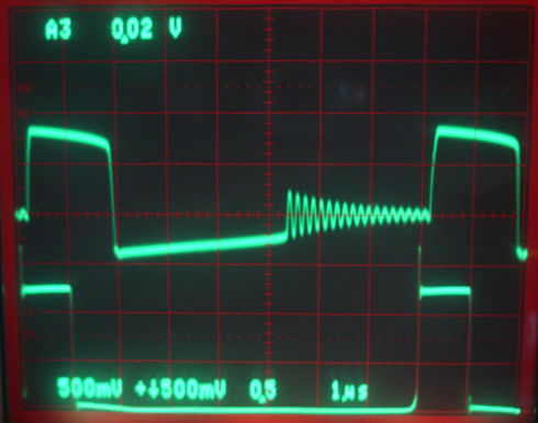
During each switching cycle of a buck regulator, the inductor goes through three phases. In the charging phase, the transistor switch is closed and the power supply charges the magnetic field of the inductor. The inductor voltage is positive and its current is increasing. The inductor charges the load capacitor. In the discharge phase, the transistor switch is open. The inductor voltage is negative and its current is decreasing. At first, the inductor continues to charge the load capacitor, but as the inductor current drops below the load current, the capacitor starts to discharge. In the harmonic phase, the inductor current is small but the voltage follows a damped harmonic oscillation the resonant frequency of the coil in parallel with its own parasitic capacitance, the diode capacitance, and the switching transistor output capacitance. During the harmonic phase, the capacitor discharges into the load. We see these three phases in the coil current trace below.
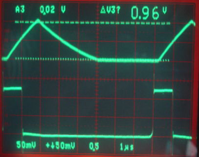
We obtained the above traces with Q1 a ZTX690A and Q2 a ZTX790A. The charging phase does not begin until 200 ns after the rising edge of the A. The typical turn-on time of the ZTX690A is 33 ns and of the ZTX790A is 35 ns. The charging phase continues for 900 ns after the falling edge of A. The typical turn-off time of the ZTX690A is 1300 ns and of the ZTX790A is 600 ns. Decreasing R1 to 100 Ω and R2 to 200 Ω has little effect upon the transition delays in our circuit.
During the charging phase, the coil current increases to 1.2 A from zero. During the discharge phase, it decreases to 0.0 A. During the harmonic phase, the current is near zero. The above traces we obtained with a 1N914 diode. When we used the larger and slower 1N4001, we obtained the following trace, where the coil current becomes negative during the harmonic stage, during the reverse recovery phase of the diode.
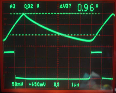
The trace below gives the voltage across the coil during one cycle. The buck regulator is in equilibrium, so the average coil current is constant. The increase in inductor current each cycle is proportional to the area under the coil voltage trace, so this area must be zero, and it appears to be so. The 1N914 capacitance is 4 pF, the ZTX790A collector capacitance is 24 pF, and the coil's parasitic capacitance is also 24 pF, so we expect the oscillations to be 7.3 MHz. We observe 6.0 MHz.
The traces below show the load voltage and switching diode voltage, which are at the coil ends. The input voltage remains a constant 10 V, which we mark on the screen with the upper dashed line. During the charging phase, the voltage across Q1 is at first small, but increases to around 1 V as the current increases. We are dissipating heat in the transistor.
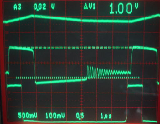
A close look at the load voltage in the above figure shows that it is increasing during the charging phase, decreasing during the entire discharging phase, and remaining constant during the harmonic phase. Our load capacitor is a 22-μF tantalum bead. We replace it with a 20-μF ceramic capacitor. The load voltage ripple drops by a factor of three. We AC-couple the ripple and increase the gain to obtain the trace below.
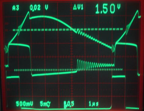
We now see the capacitor charging at 0.062 V/μs, which for a 20-μF capacitor implies a current of 1.2 A, which is correct. During the discharge phase we see the load voltage reach a peak and then start to drop. During the harmonic stage, the output capacitor is discharging at 0.025 V/μs or 500 mA.
Our average load voltage is 1.85 V. The load is a 5-Ω resistor, so we are delivering 370 mA and 680 mW. Meanwhile, we are drawing 150 mA from 10 V, so we are consuming 1.5 W. Our buck regulator is 46% efficient. Diode D1 carries an average of 600 mA for 3/8 of the time with forward voltage drop roughly 1.1 V, dissipating 250 mW. Transistor Q2 carries an average of 600 mA for 2/8 of the time with saturation voltage roughly 0.40 V, dissipating 60 mW. During switch-off, which takes Q2 around 200 ns, it conducts 1.2 A with an average of 5.0 V for 0.2/8 of the time, dissipating 150 mW. Resistor R1 carries 10 mA over 10 V for 1.7/8 of the time, for another 20 mW. The coil carries root mean square current 800 mA for 5/8 of the time with resistance 0.4 Ω, dissipating 160 mW. These losses together amount to 640 mW. Add this to the 680 mW deliver to the load and we still have 180 mW unaccounted for.
We change Q1 for a 2N4401, which has a faster switching time (turn-on 35 ns, turn-off 255 ns compared to 33 ns and 1300 ns for the ZTX690A). The delay between the rising edge of A and the turn on of Q2 decreases from 200 ns to 100 ns. The turn-off delay drops from 900 ns to 250 ns. The load voltage drops to 1.2 V and the supply current to 70 mA. Our efficiency is 41%. We switch Q2 for a 2N4403, but its current gain is only 20 at 500 mA, which is insufficient even when we drop R1 to 200 Ω. With Q2 as before, and the new Q1, we increase the switching frequency and obtain the following traces.
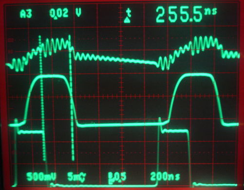
We are drawing 150 mA from our 10-V supply and delivering 1.78 V to our load, so efficiency is 42%. Here are some ideas for increasing efficiency.
[13-MAY-14] We increase VS to 15 V. Input current is 140 mA and output voltage with 5-Ω load is 2.3 V. Efficiency is 50%. Turn-off time of Q2 is 200 ns with R2 1.0 kΩ and 500 ns with 470 Ω.
[15-MAY-14] We receive the SB140-E3/54 Schottky diode. We install it as D1. The voltage across the SB140 during the discharge phase is around 0.4 V. We reduce the switching frequency to around 50 kHz. We have 3.1 V on the 5-Ω load and we are drawing 203 mA from the 15-V supply. Efficiency is 56%. Turn-off of Q2 is 550 ns after the transition on A and 390 ns after turn-off of Q1. We switch Q2 to the ZTX949. We have 3.0 V on our load and we draw 220 mA. Efficiency is 55%. Turn-off is 820 ns from transition on A and 640 ns from turn-off of Q1.
We make various changes to the circuit and measure efficiency. Ceramic capacitors for C1 had no effect. Increasing the ceramic capacitor C2 had no effect. We are using the minimum pulse width provided by our function generator, 1/8 of the period. Longer pulse lengths decrease the efficiency.
| Test | Q1 | R1 (Ω) |
R2 (Ω) |
R3 (Ω) |
Q2 | D1 | R4 (Ω) |
f (kHz) |
VS (V) |
PL (W) |
η (%) |
|---|---|---|---|---|---|---|---|---|---|---|---|
| 1 | 2N4401 | 1000 | 1000 | 120 | ZTX790A | SB140 | 5 | 63 | 15 | 1.37 | 61 |
| 2 | 2N4401 | 1000 | 1000 | 470 | ZTX790A | SB140 | 5 | 63 | 15 | 1.46 | 56 |
| 3 | 2N4401 | 1000 | 470 | 120 | ZTX790A | SB140 | 5 | 63 | 15 | 2.0 | 61 |
| 4 | 2N4401 | 1000 | 470 | 120 | ZTX949 | SB140 | 5 | 63 | 15 | 2.2 | 61 |
| 5 | 2N4401 | 1000 | 470 | 120 | ZTX949 | SB140 | 10 | 63 | 15 | 2.6 | 72 |
| 6 | 2N4401 | 1000 | 470 | 120 | ZTX949 | SB140 | 10 | 63 | 20 | 4.6 | 70 |
| 7 | 2N4401 | 1000 | 1000 | 120 | ZTX949 | SB140 | 10 | 63 | 20 | 2.9 | 64 |
| 8 | 2N4401 | 1000 | 1000 | 120 | ZTX949 | SB140 | 10 | 100 | 20 | 3.3 | 62 |
| 9 | 2N4401 | 1000 | 1000 | 120 | ZTX949 | SB140 | 10 | 50 | 20 | 3.4 | 72 |
[29-MAY-14] With 20 V, 62 kHz, R1 = 1 kΩ, R2 = 1 kΩ, R3 = 120 Ω, we are drawing 200 mA from the supply and delivering 2.7 W to our 10-Ω load. The coil terminal voltage and the switching signal are shown below.
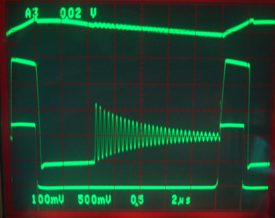
The charging phase is 1.8 μs, discharge phase is 4.2 μs, harmonic phase is 9.6 μs. The transition from charging to discharging takes place in 200 ns, the transition from harmonic to charging takes 200 ns also. Adding these together, we get the entire 16 μs switching period. We estimate the following power losses.
Adding these up we get an estimated loss of 1.7 W. Our observed loss is 1.3 W. Our calculations suggest that most of our loss is in the resistance of the coil.
[12-JUN-14] We wind the inductor shown below. The wire is copper, 1.65 mm in diameter (14 AWG copper with insulating paint). Its resistance should be 8.3 mΩ/m. The coil diameter is 28 mm and there are 40 turns, so we expect its resistance to be 0.03 Ω. Our meter says the resistance is less than 0.1 Ω.
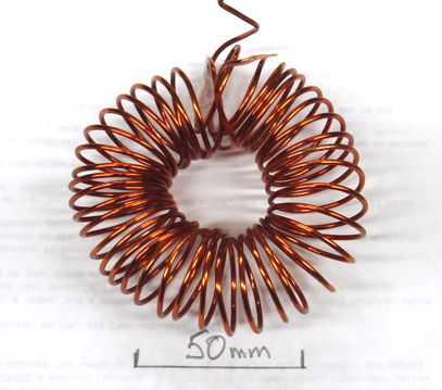
We expect the toroid inductance to be around 9 μH. We replace our original coil with this one. If our calculations of losses given above are correct, we should see efficiency improve. But it remains at 70%.
We try a 100-μH ferrite-core toroidal inductor for L1. We have 2N3904 in place of Q1, having destroyed our only 2N4401. With the higher inductance, we can reduce the switching frequency. We settle upon 16.7 kHz, with 10-μs on-time for A and 50-μs off-time. Supply voltage is 20.0 V with 140 mA, and output voltage is 4.9 V, so efficiency is 86%. Transistor Q2 is no longer hot. The only loss that is affected by reducing the switching frequency is the turn-off loss in Q2.
We resolve to try the following circuit as a way to cause Q2 to turn off more quickly, so we can use a higher switching frequency and a smaller air-core inductor.

We use an inductor and a transistor to provide a short-lived low-impedance connection between the emitter and base of Q2. The Q2 turn-on base drive is now a current sink of 27 mA rather than a saturated transistor in series with a resistor.
The above circuit reduces the switch-off time of Q2 from 200 ns to 20 ns. We find that Q2 no longer heats up. With L1 = 10 μH and 140 kHz switching, we obtain efficiency 80% and it is the coil that warms up.
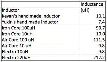
[27-JUN-14] We receive air-core inductors from Nova Magnetics. The 10-μH is 24 mm in diameter and 11 mm high. The 100-μH is 38 mm in diameter and 13 mm high. We measure the inductance of our selection of coils by resonance with 1.0 kΩ series resistance and 1 nF parallel capacitance.
[30-JUN-14] The circuit below is a prototype buck converter that obtains power from a LWDAQ root cable. A through-hole RJ-45-RS connector receives LWDAQ ±15 V power. We switch Q1 with a 3.3-V logic level referenced to 0 V. But the converter output is referenced to −15 V.
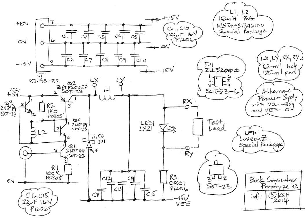
The circuit uses surface-mount transistors, diodes, resistors, and capacitors. The Schottky diode is the ZLLS2000. We allow for wire-connected inductors in place of L1 and a wire-connected load across the converter output. Michigan University tested a range of ferrite inductors and found the 74437346100 10-μH, 3-A surface-mount inductor to be effective in a strong magnetic field: its inductance is 6 μH in a 0.6-T field. We allow for this inductor to be loaded in place of L1 and L2.
We decouple the ±15 V power supplies individually with 100 μF made out of parallel P1206 capacitors. We suspect that this capacitance is great enough to bring down the ±15V power supplies at the end of a 100-m cable. We decouple the output to −15 V with another 100 μF.
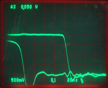
[01-JUL-14] We look at the switch-on of Q2 with 0-3.3 V logic drive. The switch-on with R1 = 100 Ω we show below.
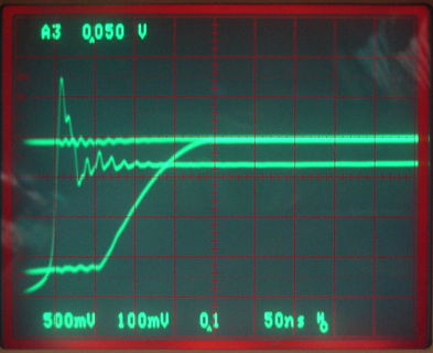
With R1 = 50 Ω we have twice the base current for Q2 during turn-on. The turn-on time drops from 100 ns to 50 ns.
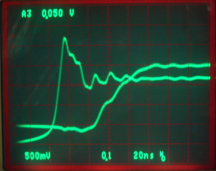
The longer turn-on time has no effect upon the converter efficiency when the inductor current drops to zero during the discharge phase. Even if we eliminate the harmonic phase by increasing the switching frequency, we still see no significant improvement in efficiency as a result of the shorter turn-on.
[30-JUL-14] Yuxin has been working on the printed circuit board prototype for the past three weeks. The photograph below shows the state it's in today. The board obtains ±15 V power from a LWDAQ cable.
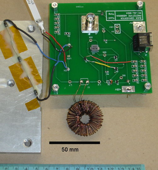
The components are as shown here, with the exception of D2, which we change to a 1N914 silicon diode, and in later versions, a silicon diode made out of a 2N3904 transistor. The purpose of D2 is to apply a charging voltage to L2 in the first few hundred nanoseconds after Q1 turns on. When we used a Schottky diode for D2, the charging voltage was reduced, so L2 took longer to charge, which increased the minimum on-time for Q1. With a silicon diode for D2, we can apply a shorter on-pulse and still get a fast turn-off.
The track lengths for component connections on this A208001A circuit board are too long for efficient switching. We added wire connections from the −15V capacitor bank and Q2 to D1. We find that an LXZ1-PR01 royal blue LED load over-heats, shorts, and damages the buck converter. We have three 1N4001 diodes in series, glued to a heat sink, as a load instead. We use a 10-μH ferrite-core surface mount inductor for L2 in the switch-off circuit. If we use 5.6 μH instead, the switch-off still works well. Given that this particular inductor has inductance 6 μH or higher for fields up to 0.6 T, we trust that our switch-off will work in fields up to 0.6 T.
At 100 kHz, we adjust the duty cycle of A so we get 1 A of load current when L1 = 10 μH. Now we drop L1 to 5.6 μH. We find Q2 starts to over-heat and the load current increases. At 100 kHz, the optimal duty cycle is 9.4%, which is roughly 1 μs of on-time. With 26 V across L1 = 10 μH, current will reach 2.6 A from a 0-A start. But with 5.6 μH, the current reaches 4.6 A. The transistor heats up and takes longer to turn off. The load current increases.
Yuxin made the coil shown above by winding wire onto a hand-made cardboard form. The coil is 30 mm in diameter and 9 mm high. By tank resonance, we measure its inductance to be 12 μH. The following graph shows the converter efficiency versus frequency, as well as duty cycle for 1-A load current. With forward current 1 A, the three 1N4001s in the load drop roughly 2.7 V.
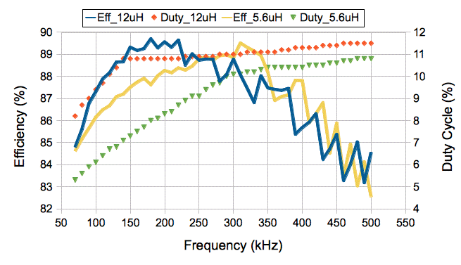
With the 12-μH air-core inductor, the harmonic switching phase vanishes at 150 kHz. Above this frequency, the inductor current is always greater than zero.
[31-JUL-14] Yuxin repeats the above measurements with a 5.6-μH ferrite-core inductor. The harmonic phase for the 5.6-μH inductor vanishes at 290 kHz. With the 5.6-μH and 10-μH ferrite-core inductors, we obtain the following graph of load current versus duty cycle at 300 kHz.
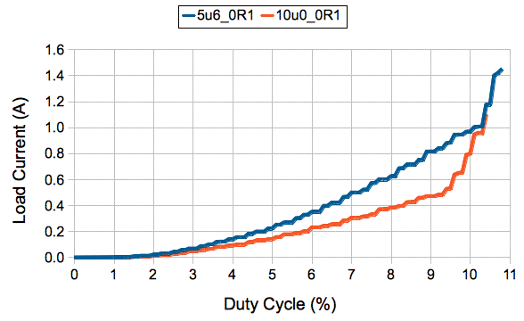
If α is the duty cycle, a perfect buck regulator will give output voltage, VO = αVI, where VI is the input voltage. In our case, we have roughly 29 V input, 10% duty cycle, and 2.8 V output. When the load is a series of diodes and 0.1 Ω, its forward current increases rapidly with voltage.
The graph below compares the efficiency of a 74437346100 10-μH ferrite-core inductor to the 5.6-μH inductor in the same family.
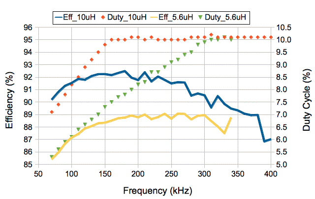
The duty cycle for 1-A output current is constant with frequency above the point at which the harmonic phase vanishes.
[28-AUG-14] Yuxin tried a variety of PNP transistors with SOT-23 packages in place of Q2. The FMMT591, PBSS4041, ZXTP25040DFH, ZXTP2025F all appear from their data sheets to be suitable for high efficiency switching in our buck converter. The FMMT591 and PBSS4041 do not appear to be able to supply 3 A with the base current available from Q1. The ZXTP24040 works okay, but tends to get hot because it takes too long to turn off. The ZXTP2025F turns off quickly and supplies 3 A easily. All our best results we obtained with this transistor.
[05-OCT-15] We are concerned about the viability of PNP switching transistors in neutron radiation. We find that their current gain decreases dramatically. The threshold voltage of p-channel mosfets is immune to neutron radiation, but is affected linearly with ionizing radiation. We have already measured the ionizing tolerance of the NDS356AP mosfet. Its threshold voltage becomes more negative by 1 V after 2 kGy. We assemble the following circuit, in which Q2 is now an NDS356AP p-channel mosfet. We drive the gate with a resistive divider and supply 30V for VIN. The inductor 5.6 μH, ferrite-core 74437346056, with resistance 43 mΩ
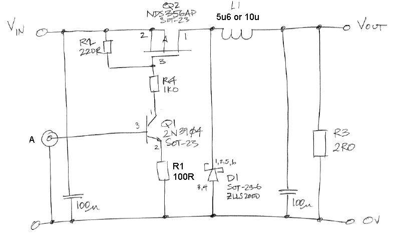
On our printed circuit board, we implement the circuit below by connecting 0V and VEE together, loading the p-channel mosfet directly into the A2 footprint, and loading R2 and R4 onto available pads. We connect a 2-Ω resistor as a load, and adjust the duty cycle of our ±3 V control signal (A) so as to bring the converter output voltage to an average of 2 V.
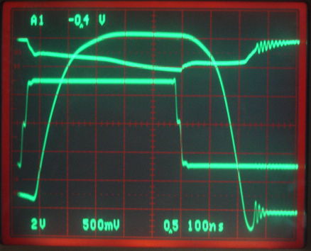
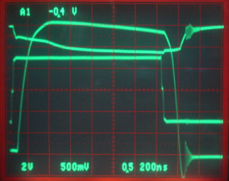
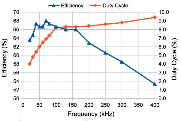
The turn-off is slowed down by the falling drain charging the gate capacitance, which is being drained by R2. We see the gate sitting at 4 V below the source for 200 ns as the drain drops from +30 V to −3 V. The Q2 package is too hot to rest a finger on. Efficiency is 67%. The lowest switching frequency at which we can obtain a 2-V output is 20 kHz. At 10 kHz, the maximum output voltage we can obtain is 1.4 V for a duty cycle of 1.4%.
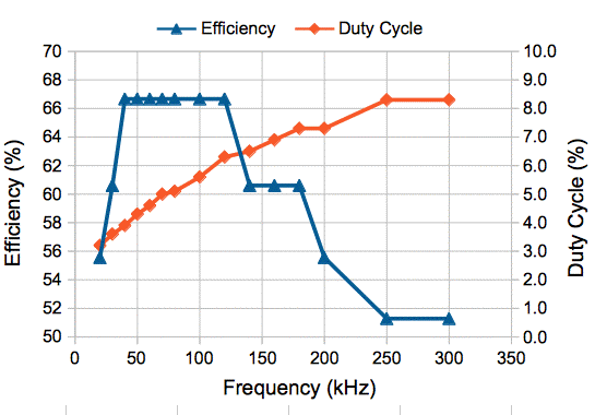
We increase frequency from 20-300 kHz, adjusting the output voltage to 2.0 V by increasing the duty cycle. We obtain the following plots of efficiency and duty cycle versus frequency.
[07-OCT-15] We reduce R1, R2, and R4 by a factor of two, so as to accelerate the turn-off of Q2. We obtain the following trace at 100 kHz. The turn-off takes about 100 ns, when previously it took around 200 ns.
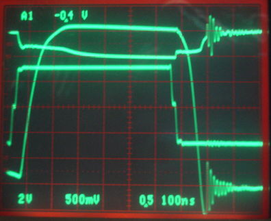
With the turn-off taking half as long, the loss in Q2 during turn-off will be halved. In the plot above, we have 30 V across 10 μH for 500 ns. The initial current in Q2 is zero, because the converter is entering its harmonic state before switch-on. The current through Q2 ramps up to 30 × 0.5 μs / 5.6 μH = 2.7 A. The turn-off puts an average of 15 V across Q2 with current 2.7 A for 100 ns. At 100 kHz that's an average of 400 mW. While Q2 is on, its channel resistance will be at most 0.3 Ω with our gate-source voltage of −5 V. With peak current 2.7 A after 0.5 μs, we get 55 mW dissipated in Q2 while it is on. We have an peak 2.7 A in L1 during the charging and discharging phases, which last for 7.5 μs of the 10-μs period. The inductor's resistance is 43 mΩ, so we have resistive loss 120 mW. The voltage across the diode is 0.6 V for 7.0 μs with average current 1.4 A, which dissipates 570 mW. The shorter turn-off comes at the cost of an increase in the current through Q1 while Q2 is turned on. Previously we had 23 mA flowing, for 0.69 W in R2, R4, Q1, and R1. Now we have 46 mA and 1.4 W. At a 6.3% duty cycle, however, this 1.4 W amounts to 90 mW. Adding the losses up we come to an estimate of 400 + 55 + 120 + 570 + 90 = 1200 mW. What we observe is 3 W in and 2 W out to the load, so our actual loss is 1.0 W. We obtain the following graph of efficiency and duty cycle versus frequency.
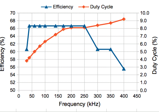
Despite the faster turn-off time, the maximum efficiency remains 67%. But we can operate at slightly higher frequencies.
[08-OCT-15] We replace the 5.6-μH inductor with 10 μH. With the larger inductor, the converter no longer enters a harmonic phase during the switching cycle at 100 kHz.
We set the frequency to 150 kHz and duty cycle to 7.5%. If our inductor were 5.6 μH we would see 2.0 V out and 67% efficiency. With 10 μH we see 1.8 V out. Input current is 86 mA for efficiency 63%. Michigan University measured the inductance of our 10-μH part in increasing magnetic fields and obtained the following results.

The maximum field we expect in the New Small Wheel is 0.6 T. Our p-channel mosfet buck converter, equipped with this 10-μH inductor, would produce 1.8 V in a 0.0-T field, and 2.0 V in 0.7 T.
We assemble the circuit shown below. We supply the circuit with 30-V power. The output capacitor is only 22 μF. The load is a LuxeonZ deep-red LED LXZ1-PA01 and a 0.1-Ω resistor.
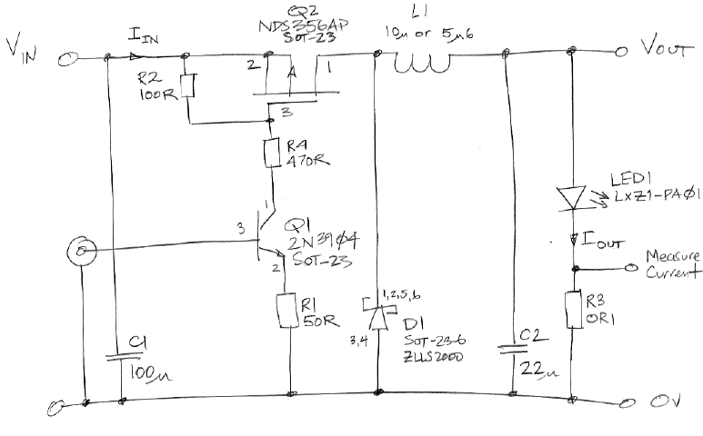
We use the voltage across the resistor to measure the output current. With L1 = 10 μH and switching frequency 150 kHz we set duty cycle to 8.7%. Load current is 800 mA, voltage 2.2 V, and 30-V input current 86 mA for efficiency 68%. After ten minutes, the LED hot. Current is 930 mA, output voltage 2.2 V, input current 98 mA for efficiency 70%. We obtain the following plots of initial load current versus duty cycle for 10 μH and 5.6 μH inductors.
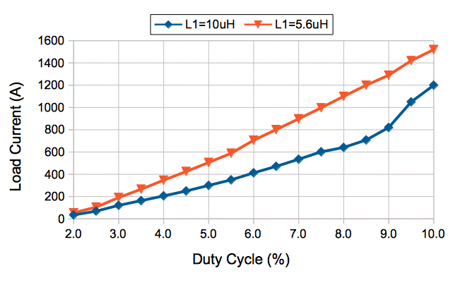
We set duty cycle to 7.5% and turn on with L1 = 5.6 μH. Current starts at 1000 mA and after five minutes is stable at 1050 mA. Components LED1 and Q2 are almost too hot to touch. We set L1 = 10μH. Initial current is 600 mA. After five minutes, current is stable at 605 mA with 30-V input current 63 mA. We try 200 kHz and 8.5% and get initial current 740 mA, settling to 830 mA with input current 91 mA. With L1 = 5.6 μA initial current is 1020 mA, settling to 1080 mA with input current 125 mA and 65% conversion efficiency.
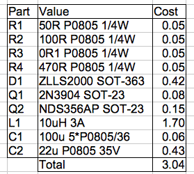
We propose to build one such buck converter for each of 36 LEDs in our contact injector. If we share the input capacitor, C1, between all 36, the component cost per converter is $3.04, half of which is the inductor. The LED is another $1.50. We turn on each LED by applying a switching signal to Q1 of its converter. We can install over-current protection on VIN, which will therefore be shared by all converters.
With 5.6 μH and 1000 mA flowing through the LED, we short the LED terminals with tweezers. In less than a second, Q2 is smoking. It fails as a short-circuit, and remains a short circuit even when we remove the switching signal from Q2. If we have 36 such converters in parallel, and one Q2 fails in this way, the entire circuit fails.
[03-DEC-15] We obtain the following plots of load current versus switching duty cycle for three inductor values. The load is a Luxeon-Z deep-red LED LXZ1-PA01.
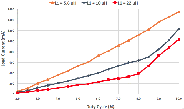
We propose to set the duty cycle to a fixed 7.5%, load the 10-μ inductor. The nominal deep-red LED current will be 600 mA. In a 0.6-T field, this current will rise to 1000 mA, which our LED can tolerate when loaded into a good heat sink.
[17-MAR-16] We propose the following buck converter prototype for use in the New Small Wheel. The circuit is designed to plug directly into the LWDAQ, with 1 μF decoupling capacitors on the ±15 V power supplies, as opposed to the 100 μF we have been using. At 150 kHz and 7.5% duty cycle, the peak current is 1.5 A into the inductor and we expect a drop of only 0.5 V across each capacitor.

We add a fuse that we hope will blow when we have a short circuit on the output or an overheat of the switching mosfet, or a failure of the switching logic signal. Instead of an NPN transistor in place of Q1, we now use an N-channel mosfet two switch the gate of Q1, and we can apply a 3.3 V logic level directly to this gate. The plan is to have one such buck converter for each LED in a 36-LED Contact Injector, and turn on each LED by applying a 150 kHz 7.5% duty cycle switching signal to S. Otherwise, S is held at zero.
[05-JUN-16] We build the above prototype. With 7.5% duty cycle the LED voltage is 2.1 V and current is 790 mA. Input voltage is 30 V and 85 mA. Efficiency is 65%.
[07-JUL-16] We note that the LWDAQ power supplies are dropping by roughly 1 V during the charging phase of our switching cycle.
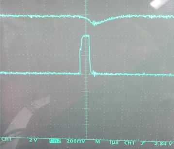
On the driver, there is a 0.47-Ω resistor in series with both the +15-V and −15-V power supplies. With a 10-μH inductor, 150-kHz switching frequency, and 7.5% duty cycle, the charging phase lasts 500 ns, during which time the inductor current reaches 1.5 A. This current, passing through the 0.47-Ω resistors, drops 0.7 V. We insert a resistor R in series with +15-V and −15-V. We consider decoupling capacitors C for both supplies, with the inductor connected directly across these capacitors with a switch. We solve for the voltage across the capacitors when we close the switch after it has been open for a long time. You will find our solution here: Page_1, Page_2, Page_3.
With a 130-m root cable, R will contain roughly 10 Ω of wire resistance, 0.47 Ω on the driver itself, and whatever value we load on the buck converter. Suppose we load 10 Ω on the converter and start with a short cable. We let C be 10 μF and L is 10 μH. The frequency of the harmonic generated by the capacitor and the inductor will be 22 kHz. During the 500-ns charging phase, we expect the capacitor voltage to drop by aroun 40 mV. With the current at 1.5 A, the capacitor voltage is dropping at 0.15 V/μs. The average current is around 60 mA, which drops 0.6 V across R. During the charging phase, this drop increases to 0.64 V. The LWDAQ power supply will see a 4 mV drop during the charging phase.
[06-OCT-16] We complete the schematic for a 36-Way Contact Injector (A2080A). The circuit uses the same bipolar transistor regulators and power switches we developed and tested for the Bar Head (A2082), as well as the LVDS transceiver. We add 1-kΩ resistors R11 and R12 across the power switches (see S2080_1). These resistors charge the 20-μF ±15-V decoupling capacitors when we plug power into the circuit. The capacitors are charged within 100 ms. When we assert WAKE, the transistor switches connect the decoupling capacitors directly to the LWDAQ cable through R12 and R13, 10-Ω decoupling resistors.
The 20-μF decoupling capacitors are each made of 10 separate 2.2-μF 100-V P1206 ceramic capacitors, C3216X7S2A225M160AB by TDK (see S2080_2. With 15-V bias, these capacitors lose 10% of their 0-V capacitance, so the total decoupling capacitance is around 20 μF for ten of them. The 10-Ω resistors isolate the LWDAQ cable from the current pulses drawn by the A2080's buck converters (see S2080_3).
The buck converters draw power during 500-ns pulses occuring at 150 kHz. During a pulse, the inductor current increases at 3 A/μs for our 10-μH inductor in no ambient magnetic field, or 5 A/μs for the same inducor in a 0.6-T ambient field. At the end of the 500 ns, the current can reach 2.5 A. At 2.5 A, the voltage on an ideal 20-μF capacitor drops at 0.12 V/μs. The current pulses seen by the LWDAQ cable should be of order 0.1 V ÷ 10 Ω = 10 mA. The LWDAQ Driver has 0.47-Ω resistors in series with its ±15-V power supplies, so we expect to see 150-kHz noise no greater than 5 mV at the LWDAQ Driver.
The average current drawn by the buck converter in a 0.6-T field is around 110 mA when we maintain 500-ns pulses at 150 kHz. The efficiency of the buck converter is 65%, input voltage is 28 V, output voltage is 2.1 V with LED current 1000 mA. The 30-V power is reduced to 28 V by the drop in the two 10-Ω resistors. The loss in the resistors is 0.2 W, which drops the total efficiency to 61%.
Once we have a printed circuit board, LWDAQ transceiver, logic chip, and enclosure, the additional cost per injector is the cost of assembling the components in this circuit.
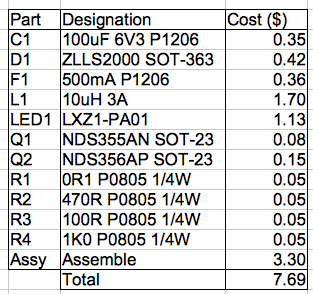
The additional cost of making a 40-way injector circuit instead of a 36-way injector circuit is around $8, not counting the extension of the face plate with hole in it for the ferrules.
[01-DEC-16] We have submitted the A208001D 36-way Contact Injector circuit board for fabrication. We have received three new types of 10-μH inductor in packages almost identical to the 74437346100, having discovered that the 7443734610 is out of stock with delivery time fourteen weeks.
| Part Number | Length (mm) | Width (mm) | Height (mm) | Core |
|---|---|---|---|---|
| 74437346100 | 7.4 | 6.8 | 2.9 | iron powder |
| SRP7028A-100M | 7.5 | 6.8 | 2.9 | carbonyl powder |
| HCMA0703-100-R | 7.3 | 6.8 | 2.8 | iron powder |
| FDSD0630-H-100M=P3 | 7.0 | 6.7 | 2.7 | metal |
Carbonyl powder is a 99.5% pure iron powder. We are not sure what "metal" is, so we cut open the FDSD0630 inductor and find that its body is entirely made of a sintered metallic powder, which we assume to be iron. To the first approximation, all four inductors have the same powdered iron core.
[19-DEC-16] We partially-assemble our first A3030A and prepare firmware P2080A01 to provide 150 kHz switching with 7% duty cycle to all thirty-six buck converters. But we populate only numbers 1, 18, 23, and 36, one example of each corner of the sets of four in which the converters are arranged. We load a different inductor in each converter. We turn on the LEDs measure current consumption, current delivered, and efficiency assuming a 30-V power supply and measuring the voltage across the LED.
| Part Number | Converter | ±15V (mA) | LED (mA) | Efficiency (%) |
|---|---|---|---|---|
| 74437346100 | 1 | 84.6 | 740 | 64 |
| HCMA0703-100-R | 18 | 78.6 | 720 | 67 |
| SRP7028A-100M | 23 | 78.4 | 710 | 66 |
| FDSD0630-H-100M=P3 | 36 | 76.7 | 710 | 68 |
When the board is asleep, it consumes 0.5 mA from +15V, 5.1 mA from +5V and 0.0 mA from −15V. When awake, but with no LED turned on, current consumption is 6.0 mA from +15V, 5.1 mA from +5V and 3.1 mA from −15 V. The +5V current consists of 1.1 mA through R1, 0.9 mA through R2, 0.8 mA through R4, and a typical 1.7 mA supply to U1 (SN65LVDM180). Those add to 4.5 mA. The current consumption of U1 may be higher than typical because our power supply is 3.5 V rather than 3.3 V.
[21-DEC-16] We turn converter No18 on and measure S18 on Q181-3, G on Q181-1, and X on Q182-1, see S2080_3. Oscilloscope traces shown below.
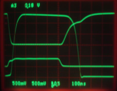
The buck converter has a charging and discharging phase, but no harmonic phase. The current through the inductor never drops to zero. The +15-V power supply average value is 14.2 V. The ripple is 60 mV. The average voltage at Q5-1 is 14.9 V and ripple is 9 mV. Between the two is R13, 10 Ω (see S2080_1), suggesting buck converter input current 70 mA. The average value of −15 V is −14.2 V and ripple is 40 mV, similar to the ripple on +15 V, but inverted. Average value at Q4-1 is −14.9 with ripple 5 mV.
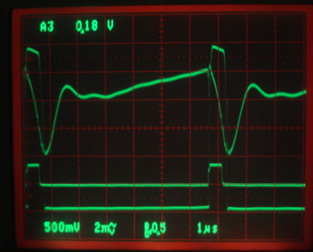
We replace R12 and R13 with 1.0 Ω (previously 10 Ω). We look at the ripple on either side of R13.

Ripple on +15V at the LWDAQ Driver (A2071E) is 7 mV and on −15V is 5 mV. The driver and the A2080A are connected by a 7-m cable. We measure 825 mA current into the LED and 2.23 V across the LED and R181 for 1.8 W delivered to the load. According to the LWDAQ power supply monitors, the current delivered on +15 V is 92.0 mA and on −15 V is 85.1 mA. According to the average voltage across R13 and R12 these currents are 89.3 mA and 89.8 mA respectively. Assuming an exact ±15 V in the LWDAQ Driver, both measurements give us 68% efficiency in the buck converter.
We reduce the duty cycle of our switching signal from 7% to 0.6%. Each pulse is 40-ns long in a period of 6.5 μs.
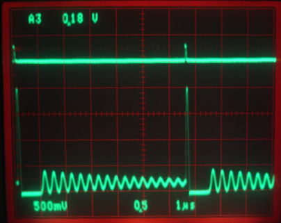
The P2080A01 firmware allows us to drive a single LED at full or medium power, and all LEDs simultaneously at low power. The current in LED No18 immediately after turning on is roughly 800 mA at full power, 580 mA at medium power, and 40 mA in low power. We have four LEDs loaded on our prototype and ±15V current is 30 mA when all four are running at low power. We expect 300 mA to turn on all thirty-six LEDs at low power, allowing us to see if all are operational at one time.
[22-DEC-16] Commands sent to the A2080A with firmware P2080A01 produce the following effects.
| Command (Hex) |
LEDs On | LED Current (mA) |
Converter Current (mA for all) |
Comment |
|---|---|---|---|---|
| 0000 | None | 0 | 0 | Asleep, ±15V connected through R10 = R11 = 1 kΩ |
| 0080 | None | 0 | 0 | Awake, ±15V connected through R12 = R13 = 1 Ω |
| 0181 | No1 | 900 | 86 | No1, deep red, full power. |
| 0182 | No1 | 600 | 64 | No1, deep red, medium power. |
| 0182 | No1 | 660 | 84 | No1, green, high power. |
| XX83 | All | 40 | 220 | All 36 deep red, low power, calculated from 24 mA for 4 LEDs. |
| 1282 | No18 | 800 | 85 | No18, deep red, high power. |
| 1782 | No23 | 830 | 83 | No18, deep red, high power. |
| 1782 | No23 | 610 | 81 | No18, cool white, high power. |
| 2482 | No36 | 830 | 82 | No36, deep red, high power. |
In the case of the green LED in location No18, the full-power current is 660 mA with forward voltage 2.76 V for efficiency 72%. The cool white in No23 has current 610 mA and forward voltage drop 2.97 V for efficiency 74%.
[17-JAN-17] We have two pot magnets from Radial Magnet Inc., part number A32 made out of N35 neodymium. This material generates a surface field of roughly 1.2 T. The field is strongest in an annulus 3 mm thick on the underside of the magnet. We place this field on L011. The magnet sticks to the inductor.
| Configuration | +15V Input (mA) | Comment |
|---|---|---|
| All lamps off, awake | 0 | Baseline current. |
| No1 full power, no magnet | 90 | Stays on indefinitely. |
| No1 full power, with magnet | 220 | Fuse blows after one second. |
| No1 2/3 power, no magnet | 63 | Stays on indefinitely. |
| No1 2/3 power, with magnet | 160 | Fuse blows after a few seconds. |
| All 4 at 0.7% power, no magnet | 6 | All four at low power. |
| All 4 at 0.7% power, magnet on No1 | 14 | No1 gets brighter. |
When we apply the magnet to L011, the current through the deep-red No1 LED increases. At 0.7% power, the increase is 6 to 14 mA, at 67% it is 63 to 160 mA, at 100% it is 90 to 220 mA, which is a factor of 2.3, 2.5, and 2.4. It appears that the effective inductance of L011 drops by a factor of 2.4 in 1.2 T, resulting in an increase by the same factor in the peak current reached during the charging period. The effective inductance is now 4.2 μH instead of 10 μH. We are unceratin of the magnetic field strength, but have asked the manufacturer of the magnet for a field map. The L011 inductor is 74437346100, the magnet tested by University of Michigan at 0.6 T, at which field it had an effective inductance of 5.6 μH.
[18-JAN-17] We have seven 13-mm diameter, 3.2-mm thick N35 disk magnets, part number 8022 from Radial Magnet Inc.. At K&J Magnetics we find a field-mapping calculator for such magnets, and obtain the following for a single disk and for seven disks in a row.
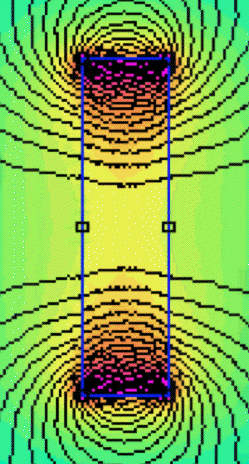


The field is stronger at the perimeter of the end face than at the center. In the case of one disk, the field at the center of the end face is 0.30 T and at the perimiter is closer to 0.5 T. For seven disks, the field at the center is 0.63 T and at the edge is closer to 0.7 T. When we stick the magnets to our inductor L011, the pull force is stronger when we place the perimiter of the magnet over the center of the inductor. We measure the additional current consumption that results from turning on LED No1 to 2/3 power for various arrangements of magnets.
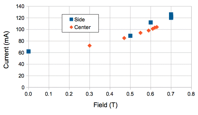
It appears that the current doubles for a field of 0.7 T, which suggests the effective inductance of L011 has dropped to 5 μH from 10 μH.
[19-JAN-17] Our Injector LED Test Board (A2080Z) provides footprints for sixteen Luxeon Z LEDs, a 5-V power supply, and sixteen MOSFET switches to turn them on and off, which we can in turn connect to a Multi-Purpose Device (A2081) to implement individual control of the LEDs. Schematic is S2080Z_1, views of assembly A2080Z_1 and A2080Z_2.
[06-FEB-17] We assemble a fiber-mounting plate onto a circuit board with thirty-six LEDs. Most are red, but some are green, blue, white, and yellow. We fit a fiber tip into one of the mounting holds. It is roughly 1 mm from the LED, and the LEDs are centered to ±0.5 mm. We turn on to full power and measure power at the other end of the optical fiber. For six red LEDs we 42-50 μW. With a white LED the photodiode current is 16 μA, which suggests a total power of around 70 μW.
[15-FEB-17] We use an SD445 photodiode and 1% neutral density filter to measure the power emitted by LED No36 on our December prototype. We have firmware P2080A03, which supports ten power levels.
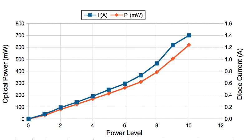
At 1.4 A diode current, the voltage across the diode and sensing resistor is 2.25 V and current drawn from the ±15 V supply for the converter is 174 mA. The voltage delivered to the converter is 29.5 V. The converter efficiency is 61%. The diode emits 620 mW of light while consuming 3.0 W of electrical power, for an optical efficiency of 21%.
[16-FEB-17] We note that the −15 V decoupling capacitors C18-C27 do not discharge after we unplug the circuit board from the LWDAQ, while the +15 V capacitors C8-C17 discharge in less than a second. The +15 V capacitor is a total of 22 μF discharging through R3 of 22 kΩ for a time constant of 500 ms. With all buck converters off, the −15 V capacitor discharges through the leakage current of thirty-six mosfets and diodes. We see the voltage drop to 13 V in roughly 100 s, suggesting a total leakage current of around 500 nA. We add R14, 22 kΩ from −15 V at its input to 0 V.
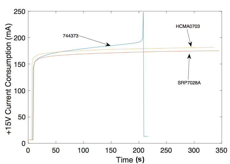
[30-MAR-17] We have a permanent magnet that generates a field of 450 mT in a cylindrical volume 25-mm long and 25-mm in diameter. We place the buck converter inductor in this field at power level 7. The fuse blows immediately when we have FDSD0630-H-100M in place of Ln1, but not for the other three inductors. We measure total LWDAQ +15-V current versus time for the other three inductors in 0 mT and 450 mT. The 74437346100 blows the fuse after 200 s in no magnetic field. We have no heat sink attached to the A2080A circuit board.
We repeat the same experiment in a 450 mT magnetic field.
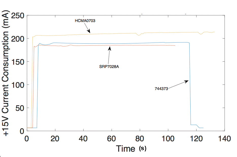
The FDSD0630 blows the fuse immediately in 450 mT and the 744373 blows the fuse after 120 s. We reject both of these inductors for our A2080A. The SRP7028A-100M current does not change significantly with time, either at 0 mT or 450 mT. The HCMA0703-100-R performs well also, but its current increases from 175 mA to 210 mA. We choose the SRP7028A-100M for our A2080A assembly.
[03-APR-17] When we send a command of the form xxB0 to the A2080A, its current consumption, as measured by the Diagnostic Instrument, increases as high as 1000 mA.
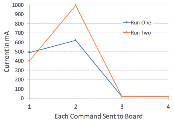
We find a vulnerability in firmware P2080A03.abl. When we send a command with power level zero following a command for which the power level is not zero, there is a chance that a switching signal for one of the buck converters will be stuck HI, causing the LED to flash and the LWDAQ power supplies to be brought down without blowing the fuse. We fix this vulnerability in P2080A04.abl.
[27-APR-17] When an LED is damaged, or loaded imperfectly, it can act like an open circuit. When we turn on the buck converter, Cn1 charges up to 30V. If Cn1 is rated at 6.3 V it may fail open-circuit or closed-circuit. We load 10 μF 35V in place of C011 and obtain the following trace for ripple on the LED voltage (Y) for power level 7 and Rn1 = 0.1 Ω.
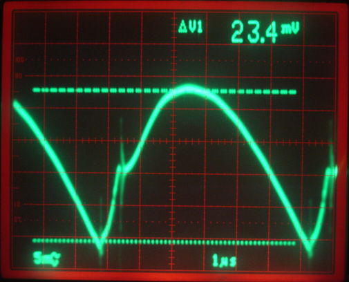
The total ripple is 230 mVpp, while for 100 μF it is around 30 mVpp. The charging phase of the cycle is the steepest vertical ascent from the minimum. The current out of the capacitor towards the end of the cycle is 10 μF × 0.1 V / 1.2 μs = 830 mA. We look at X for power levels 1-7 and note that the harmonic phase of the buck converter cycle vanishes at power level 7, but we assume the current in the inductor is close to zero at the end of the cycle. In the cycle above, it appears that the minimum current is 830 mA. We note that the capacitor is only ±20% accurate. The current drawn from ±15V is 93 mA with 10 μF and 91 mA with 100 μF, as measured by the driver's power monitors.
[08-MAY-17] We change Cn1 to 22 μF 35 V on the schematic and BOM. This is the largest capacitance value we can find in a P1206 package with 35-V rating. We choose this capacitor.
[05-JUN-17] We use this script to send random commands to a contact injector while measuring current consumption to see if we can break or damage the board, or set it into an irreversible state. No such problems arise. We load 36 of LXZ1-PA01 deep red Luxeon-Z LEDs onto three boards. We measure LED forward current and optical output power for all LEDs. Current varies 600-800 mA and output power 230-310 mW. Higher current usually corresponds to higher current, but not always. We turn on an LED and let it warm up without the injector base plate to act as a heat sink. Over two minutes, forward voltage drops from 2.0 V to 1.9 V, output power increases from 215 mW to 235 mW and LED current increases from 820 mA to 880 mA. The current drawn by the buck converter from ±15 V drops from 75.0 mA to 74.5 mA. The efficiency of the converter, in terms of optical output power per watt drawn from ±15 V, increases as the LED warms up.
We have ten of A2080A from our assembly company. An accidental deletion in the layout of the A208001E printed circuit board has left eight injectors without +15 V power. Two wire links between +15V test points restore power and all thirty-six LEDs work.
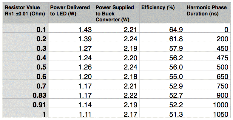
[19-JUN-17] We measure the effect of increasing the current sense resistor, Rn1, from 0.1 Ω to 1.0 Ω with 100 μF for Cn1. Our hope is to increase the duration of the harmonic phase so as to stabilize the circuit for small changes in LED forward voltage and significant drops in inductance when we insert the converter into a magnetic field of 400 mT.
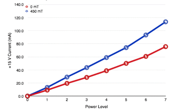
[27-JUL-17] We measure current consumption of the buck converter with increasing power level in and out of our magnetic field.
[17-AUG-17] We find that the LEDs on our injectors are on average 0.25 mm too low as shown in the photograph below. It appears that we centered the LED package on the ferrule holes instead of the LED emitting surface.
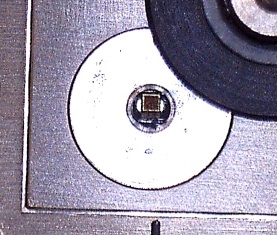
The LED must be within 0.25 mm of the center of the ferrule hole, or else the numerical aperture of the 62-μm NA = 0.22 fiber will not be contained entirely upon the LED emitting surface.
[07-SEP-17] We have a new MF100 magnetic field sensor. We measure field strength parallel to the axis of the SRP7028A-100M solenoid as we move the buck converter on a micrometer stage in and out of our horseshoe magnet. We turn the buck converter on to power level 7 and record the
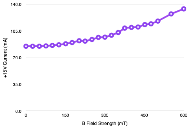
According to the new sensor, the peak field in our magnet at the edges of the poles is 600 mT. From 0 mT to 600 mT the converter current increases by ×1.7, which suggests the effective inductance of L1 has decreased to around 6 μH.
We irradiate an A2080A with fast neutrons to a dose of 14 Tn. When we turn on the LED for the first time at power level 7, the power we get on the other end of a fiber is 22 μW, while we expect 35 μW from an un-irradiated board. After 10 min, the power has risen to 27 μW. The next day, it is 27 μW at time 0 min, and 29 μW after 2 min. Three days later it is 27 μW after 2 min. When we replace the LED, the buck converter input current is within a few percent of that of an un-irradiated converter.
[18-DEC-17] We complete our study of inductors in strong magnetic fields. According to Mr. Li's work, the A2080A can tolerate up to 0.5 T running at Power Level 7. We complete our LED placement errors in our A208001E printed circuit board. We move the LEDs in the A208001F circuit board to conform with Ms. Rigger's recommendations.
[12-FEB-18] We measure the location of ferrule hole centers with respect to the nominal center of the LED package on the A2080B that uses our new red A208001F printed circuit board combined with the existing face plate. We present our results in this report (Kimberly Rigger). On average, our LEDs are 170 μm left of center and 75 μm too low. But the centering is consistent to ±50 um across all LEDs and a sample of six boards. As the report shows, we are still certain to obtain >95% of the ideal light injection.
[01-MAR-18] We generate P2080A05.jed so that all registers of the LC4128ZE logic chip power up in the reset state, and all outputs are slow-slew with level holding. Our hope is that the logic chip will power up in a defined, reset state.
[19-APR-18] Based on the blank red injector boards before assembly, we measured an expected displacement of 170 um horizontally and 70 um vertically between the centers of the LEDs and the centers of the ferrule holes. Based on 5 measurements of one of our newly-consturcted boards from Advanced Assembly, we measured an average of 185um horizontally and 55 vertically.
[27-APR-18] We have nine A2080B assembled with face plates. We take the same optical fiber jumper and turn on each of the 9 × 36 = 324 LEDs on to full power (800 mA, power level 7, firmware version 5). We measure the power coming out of the other end of the fiber. We are using S705T-02F-62N3, 62-μm core, 125-μm cladding, NA=0.275 radiation-tolerant fiber with a 2.5-mm diamater zirconia ferrule.
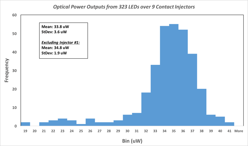
One LED burned out before we could measure power. Thirty-six are below 30 μW, and all these are on the same A2030B circuit board. The rest have average power 35 μW, which is what we expect from our calculations. We later replace a transistor on the one poorly-performing A2080B and its thirty six LEDs produce average power 35 μW.
[25-JUL-18] We test 210 new A2080B circuits. Ms. Rogers reports, "One of the injectors had a broken transistor (Q2) which caused it to have lower than normal power outputs. Another had a broken logic chip which wouldn't send commands to one of the LEDs. Two of them had a broken LED. The last broken injector had two dry pins out of the three on one of the transistors on the LWDAQ interface." That's a total of five boards with problems out of 210. Given that each board has 452 parts, we are well-satisfied with the reliability of our assembly house.
When we transmit command "0107" to the A2080B, LED No1 turns on, even though the WAKE bit is cleared and the board is supposed to be asleep. Current for the buck converter is passing through resistors R10 and R11. The +/-15V power supplies from the driver remain +/-15V at the connector. Across R10, the voltage rises from -15V to -9V. Across R11, the voltage drops from +15V to +7V. We appear to be delivering 8 mA to the buck converter from +15V and 6 mA from −15V.
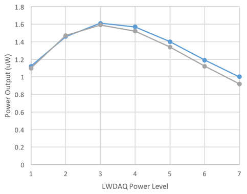
The power emitted with command "0107" is roughly 3% of the power emitted by "0187". In the plot above, we see 1 μW of red light injected into a fiber for "0107". In the same arrangement, we see 35 μW with "0187".
[13-FEB-19] We have shipped 200 of A3028B to CERN. We will perform quality control upon these circuits at CERN using a procedure we describe in detail in our Quality Control package, which includes a PDF guide to setting up a test stand to measure the power output of all thirty-six LEDs at once, a spreadsheet to record the power measurements, and two scripts for use with LWDAQ to run the test.
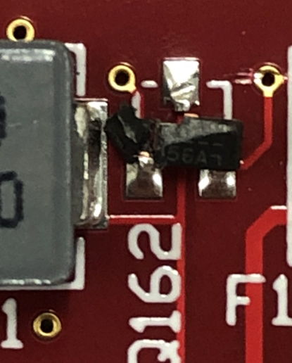
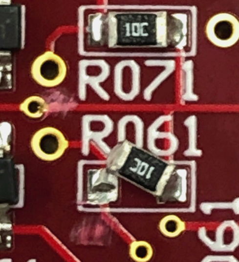
[01-MAY-19] We have returned from CERN three faulty A2080B circuits in their housings. All of these passed through our power meausurement and burn-in tests at Brandeis. Injector 00165: C7 LED does not turn on. Cause: Q162 NDS356AP transistor broken (visible physical damage). Injector 00076: D4 LED does not turn on. Cause: R061 resistor visibly dislodged. Injector 00170: Only C5 LED turns on and is far brighter than a properly working LED is expected to be, no matter which command is sent. Cause: Q122 NDS356AP transistor broken (visible physical damage).
[05-DEC-19] The Deep Red Luxeon Z LED, part number LXZ1-PA01, is being made with a new die, as announced in this change notice. It could be that the light distribution across the LED surface is no longer consistent with our original maps.
[14-JUN-21] We examine injectors and multiplexers returned from CERN and conclude that the bottom sides of the circuit boards have been damaged by contact with the locking knobs of other injectors upon which they have been stacked. Xinfei Huang presents the damages and its correlation with knob position in this report.
[15-DEC-22] Back in 2020 some technicians at CERN drilled holes in the steel JD disk. Metal chips fell down upon the equipment below, entering sockets on our multiplexers and penetrating the enclosures of our contact injectors. Over the next two years, we made every effort to clean the sockets and surroundings of our electronics, but we have nevertheless lost half a dozen multiplexers and a dozen contact injectors, as well as a few BCAMs to short circuits caused by metal fragments.
[20-JAN-23] We have a box of A2080B injectors returned from CERN, all broken or in need of inspection. Most we believe have been damaged by metal chips, but some may have residual problems from physical damage during shipping in 2019. Calvin tests them and reports as follows. "Attached are my results for the testing of the injectors. As you will see, I found all but two of them to have very similar symptoms. I did find metal shavings in several of them once the cases were removed." Table of test results here.
[24-MAY-24] We have ten red A2080B and two green A2080A injectors back from CERN. The A2080A just need re-programming with the latest element number allocations. The others have various problems. Most common is one of the NDS356AP switching mosfets has burned out as a short circuit. Its LED is always on. Replacing the NDS356AP fixes the problem. No027 has a damaged logic chip: several switching outputs are not driven and reprogramming does not cure. Physical problems are as follows.
[29-MAY-24] On each of No157, No090 we replace Qn2 on all LEDs that are stuck on. We find that no LEDs will turn on after this. We reprogram U4 and the board is fully functional. This is one of the first absolutely clear examples of a logic chip forgetting its program after external short-circuits applied to its outputs. On No027, we replace U4, program, and all is perfect. All of our injectors are now working except for one, which needs a fuse replaced.
[24-JUN-24] All injectors working.
[01-AUG-24] We are deploying the A3080A/B in our Direct Fiber Positioning System (DFPS). The fiber view cameras are 310 mm from the fiber sources, and the fibers are 100-μm in diameter. At power level 1 and exposure time 0 us, the injectors are saturating our image sensors. We update the firmware so that power level 7 remains maximum power, but power level 1 is very much less. We now have firmware P3080A07. Will measure relative power output of the seven power levels tomorrow.
[02-AUG-24] We place an SD445 photodiode over the ferrule hole of A1 on injector C0622, an A3080A. We program with P2080A07. We measure photocurrent versus power mode.

We try power level one with our DFPS and the images are still saturating even with zero flash time.
[17-AUG-24] We find a bug in the P2080 firmware: when a command is incoming, we have Command Active (CA) asserted, which clears the switching counter to zero, for which the boost converter switch turns on. When we turn on a lamp, it turns on to the correct brightness. When we turn it off, the buck converter switch will turn on for the entire duration of command reception, which is 10 μs. During that time, we have 28 V across the 10-μH buck inductor. With ±15 V remaining stable, the inductor current would rise to 30 A. In practice, the current will be limited by the cable resistance from the driver. Today, however, we blew a fuse in one converter with a 1.5-ft cable from the driver. We tried to blow other fuses with the faulty firmware, also with short cables, but failed. We fix this bug. Now we find that our fiber-view cameras do not saturate, even with power level seven, until exposure time is 1 ms.