 Bar Head (A2082) Manual
©2015-2021, Kevan Hashemi, Brandeis University© 2022-2023, Kevan Hashemi, Open Source Instruments Inc
The Bar Head (A2082) is a LWDAQ device that provides readout for four ICX424 image sensors, readout for four 1000-Ω RTD sensors, and control of four LED arrays. The four images sensors connect via two extension arms, each of which plugs into a twelve-way flex socket on the A2082. The A2082A we designed for use in the ATLAS nSW alignment bars.
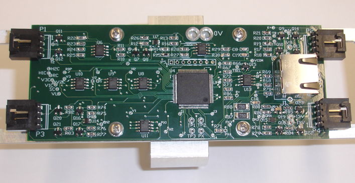
The four image sensors are mounted each upon their own ICX424 Minimal Head (A2076). In the nSW alignment bars, we use four of the A2076F. They each connect to an extension arm with a 12-way 1-mm pitch flex cable. Each extension arm connects to the A2082A with a 12-way 1-mm pitch flex cable also. The RTDs connect in pairs to four-way plugs. The LED arrays also connect in pairs to four-way plugs. No damage will be done to the A2082A if we connect LED arrays to its RTD plugs or RTDs to its LED array plugs.

The 12-way flex sockets on the A2082 Bar Head and A208201 Extension Arm are surface-mount connectors with contacts only one one side: the side farthest from the circuit board. Thus we insert the flex cable with its terminating contacts facing away from the board, in which orientation they are visible to us as we insert the cable in the socket.
[28-APR-22] The A2082 is a LWDAQ device of type ICX424 (6) when we read it out one pixel at a time, and device type ICX424Q (7) when we read it out with quadruple pixels. When we flash one of its LED arrays, we can use device type ICX424 (6) or ICX424Q (7), because these have the same allocation of bits for flash jobs. The A2071E and A2037E LWDAQ Drivers support both device types, but you will need firmware version 6+ for the A2071E and 18+ for the A2037E. The following table shows the command bit allocation for the enhanced ICX424 and ICX424Q device types. The enhanced device types are backward-compatibile with the original ICX424 and ICX424Q device types in earlier versions of the LWDAQ Driver firmware. Thus we can, with the enhanced device types in the new firmware, still operate older ICX424 devices such as the Laboratory Camera (A2075A) and HBCAM Head (A3025A).
| VDS | DC16 | DC15 | DC14 | DC13 | DC12 | DC11 | DC10 | DC9 | DC8 | DC7 | DC6 | DC5 | DC4 | DC3 | DC2 | DC1 |
|---|---|---|---|---|---|---|---|---|---|---|---|---|---|---|---|---|
| 0 | PXBN | 0 | 0 | ON4 | ON3 | ON2 | ON1 | CCD1 | WAKE | LB | SUB | V3 | V2 | V1 | H | RDP |
| 1 | X | 0 | 1 | T8 | T7 | T6 | T5 | T4 | WAKE | LB | X | T3 | T2 | T1 | TT | TB |
| 2 | X | 1 | 0 | X | D7 | D6 | D5 | D4 | WAKE | LB | DRX | DTX | D3 | D2 | D1 | D0 |
| 3 | PXBN | 1 | 1 | ON10 | ON9 | ON8 | ON7 | CCD3 | WAKE | LB | SUB | V3 | V2 | V1 | H | RDP |
The DC15 and DC14 bits are called VDS1 and VDS0 respectively. They determine the Virtual Device Select number, or VDS. The enhanced ICX424 and ICX424Q device types provide four virtual devices. Two are dual-CCD, quad-source cameras, one is an octal thermometer, and one is a data device. In an ICX424 device that does not implement the virtual devices, VDS1 and VDS0 may be used for ON6 and ON5, as they were in the HBCAM Head (A3025). We cannot use ON5 and ON6 to drive light sources if we want to use VDS0 and VDS1 as the virtual device select number. When we select one of the virtual devices, we set all fourteen of its control bits. Some may be in use, others are not. When we select another of the virtual devices, these fourteen control bits are reset to values that put virtual device into a benign state. By benign state we mean a state that will not draw excessive current from the power supplies, will not cause any amplifiers to saturate, will not cause disruption of an accumulating image, and will not leave a light source shining. The following table gives the benign values of all control bits.
| VDS | DC16 | DC13 | DC12 | DC11 | DC10 | DC9 | DC8 | DC7 | DC6 | DC5 | DC4 | DC3 | DC2 | DC1 |
|---|---|---|---|---|---|---|---|---|---|---|---|---|---|---|
| 0 | PXBN | 0 | 0 | 0 | 0 | 0 | WAKE | LB | 0 | 1 | 1 | 1 | 0 | 0 |
| 1 | X | X | X | X | X | 0 | WAKE | LB | X | 0 | 0 | 0 | 0 | 1 |
| 2 | X | X | X | X | X | X | WAKE | LB | X | X | X | X | X | X |
| 3 | PXBN | X | X | X | X | 0 | WAKE | LB | 0 | 1 | 1 | 1 | 0 | 0 |
The PXBN bit enables pixel binning to produce quadruple-sized pixels. The V1-V3 bits control the three vertical phases of the IXC424. With VDS = 0, the device provides readout for two image sensors and control of four light sources. When we assert the CCD1 bit, we select image sensor No1. Otherwise we select sensor No2. When we assert ON1-ON4 we turn on sources No1 to No4. With VDS = 1, the device becomes an octal thermometer. We select the top and bottom reference resistors with TT and TB. The eight sensors we select with T1-T8. With VDS = 2, the device transmits a data byte when we assert DTX, and it accepts eight bit data on DC1-DC4 and DC9-DC12 when we assert DRX. With VDS = 3, the device provides readout for two image sensors and control of four light sources. When we asert the CCD3 bit, we select sensor No3. Otherwise we select sensor No4. When we assert ON7-ON10 we turn on sources No7 to No10.

The A2082A does not implement all possible functions of the enhanced ICX424 and ICX424Q device types. The table below gives the device bit allocations we implement in the A2082A as a function of virtual device select number.
| VDS | DC16 | DC15 | DC14 | DC13 | DC12 | DC11 | DC10 | DC9 | DC8 | DC7 | DC6 | DC5 | DC4 | DC3 | DC2 | DC1 |
|---|---|---|---|---|---|---|---|---|---|---|---|---|---|---|---|---|
| 0 | PXBN | 0 | 0 | ON4 | ON3 | ON2 | ON1 | CCD1 | WAKE | LB | SUB | V3 | V2 | V1 | H | RDP |
| 1 | X | 0 | 1 | X | X | X | X | T4 | WAKE | LB | X | T3 | T2 | T1 | TT | TB |
| 2 | X | 1 | 0 | X | X | X | X | X | WAKE | LB | X | X | X | X | X | X |
| 3 | PXBN | 1 | 1 | X | X | X | X | CCD3 | WAKE | LB | SUB | V3 | V2 | V1 | H | RDP |
To read out the third and fourth image sensors in single-pixel mode, we tell the driver the device type is ICX424 and we set the device element to 3 and 4 respectively. The driver implements the virtual device selection automatically, based upon the image sensor number we wish to read out. If the A2082A had light sources 7 through 10, the driver would likewise set the virtual device select number to 3 when we set the device element to 7 through 10 on a flash job.
[04-MAY-15] The following table shows how current consumption varies with the state of the board and the ionizing radiation dose.

We expect the following current consumption from +15 V with no image sensors attached: 6 mA for the power supply switch, 1 mA for the thermometer current generator, 32 mA for fourteen op-amps, and 6 mA for the analog switch. We expect a total of 45 mA and we observe a total of 50 mA. From −15 V we have 0 mA for the thermometer current generator and only 3 mA for the power supply switch, so we expect 41 mA and we observe 42 mA. The CCDs are attached only to +15 V. They appear to consume around 6 mA each.
[25-JUN-15] The following table shows the quiescent current of several un-irradiated circuits with no sensors or sources attached.
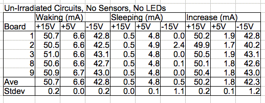
[29-JUL-20] We have the following current consumption signatures in the Analyzer Tool database. The A2082-L is the circuit fully-loaded with four image sensors and four blue LED arrays. The A2082-B is the bare circuit with no sensors or LED arrays. The A2082-P is partially-loaded with one image sensor (CCD1) and one red LED arrays (LED1).
A2082B-L:
loopback yes
termination yes
0   0 0 0.0 0   0 increase_with_0000
0  74 0 1.8 0  40 increase_with_0080
0   0 0 0.0 0   0 increase_with_0001
0 108 0 2.1 0  74 increase_with_1080
0 108 0 2.1 0  74 increase_with_0480
0 108 0 2.1 0  74 increase_with_8280

:A2082B-B:
loopback yes
termination yes
0   0 0 0.0 0   0 increase_with_0000
0  49 0 1.8 0  42 increase_with_0080
0   0 0 0.0 0   0 increase_with_0001
0  50 0 2.1 0  42 increase_with_1080
0  50 0 2.1 0  42 increase_with_0480
0  50 0 2.1 0  42 increase_with_8280

:A2082B-P:
loopback yes
termination yes
0   0 0 0.0 0   0 increase_with_0000
0  74 0 1.8 0  40 increase_with_0080
0   0 0 0.0 0   0 increase_with_0001
0  60 0 2.1 0  50 increase_with_1080
0  60 0 2.1 0  50 increase_with_0480
0 110 0 2.1 0 100 increase_with_8280
Waking up the board turns on all the ±15V power supply. The power supply switch consumes 7 mA from +15V and 3 mA from −15. The op-amps consume tens of milliamps together, and the thermometer current source draws a few milliamps from +15V. The total current is 49 mA from +15V and 42 mA from −15 when no peripheral components are attached to the Bar Head. When we add four image sensors (CCDs), they consume another 25 mA from +15V only. With command 0x1080 we turn on LED array number one. If the array is blue, it will draw around 35 mA, if red then 50 mA. The array current adds to ±15V.
[09-APR-15] The saturation level of our image sensor readout is the intensity of pixels that connot hold any more charge. In our LWDAQ eight-bit images, the intensity is a number betwen 0 and 255. The black level is the intensity we get when we have no light on the image sensor. The dynamic range is the difference between the saturation and black levels. The A2082A provides single-pixel and quadruple-pixel readout of the ICX424. The table below gives the saturation level and dynamic range for various cable lengths, resistor values, and radiation doses. We measure the saturation level by holding a lens over the image sensor and taking pictures of our computer screen. We measure black level by covering the image sensor with a black cloth.
| Image Sensor |
Readout Type |
Radiation Dose |
Cable Length (m) |
Rs (Ω) |
Saturation Level |
Dynamic Range |
|---|---|---|---|---|---|---|
| 0_1 | Single | 0 | 2 | 390 | 110 | 69 |
| 0_1 | Single | 0 | 2 | 100 | 227 | 180 |
| 0_1 | Single | 0 | 80 | 390 | 98 | 57 |
| 0_1 | Single | 0 | 120 | 390 | 97 | 56 |
| 0_2 | Single | 0 | 120 | 390 | 109 | 77 |
| I_1 | Single | 500 Gy | 120 | 390 | 118 | 48 |
| I_2 | Single | 500 Gy | 120 | 390 | 117 | 42 |
| N_A | Single | 2 Tn | 120 | 390 | 73 | 24 |
| N_G | Single | 14 Tn | 120 | 390 | 140 | 27 |
| 0_1 | Quadruple | 0 | 2 | 390 | 228 | 90 |
| 0_1 | Quadruple | 0 | 2 | 100 | 255 | 216 |
| 0_1 | Quadruple | 0 | 80 | 390 | 178 | 139 |
| 0_1 | Quadruple | 0 | 120 | 390 | 176 | 136 |
| 0_2 | Quadruple | 0 | 120 | 390 | 151 | 110 |
| I_1 | Quadruple | 500 Gy | 120 | 390 | 120 | 40 |
| I_2 | Quadruple | 500 Gy | 120 | 390 | 117 | 31 |
| N_A | Quadruple | 2 Tn | 120 | 390 | 72 | 20 |
| N_G | Quadruple | 14 Tn | 120 | 390 | 142 | 11 |
Irradiated image sensors have dark current that fills up the image pixels as they are read out. Their black level is the same as a non-irradiated image sensor at the top of the image, and higher at the bottom. For such sensors, we use the average intensity of a zero-second exposure in the dark as our black level to calculate dynamic range.
When we drop R70 and R86 to 100 Ω, we increase the saturation level for single-pixel readout. The saturation level for quadruple-pixel readout with a fresh sensor is now far above the range of our ADC, as we noted previously.
[09-JUL-15] The A2082 provides connection to four resistive sensors. The readout procedure is identical to that of the A2053. The Thermometer Instrument provides readout of the A2082 when we enter "A2082" for daq_device_name. We can select any one of these four sensors for readout, or one of the two reference resistors loaded on the circuit board itself. The Top Reference Resistor (RT) is the R17 + R18. The Bottom Reference Resistor (RB) is the sum of R19 + R20 + R21. The selected resistor receives the drive current from Q7. In the A2082A we have R10 = R11 = 2.0 kΩ, which sets the drive current at 330 μA, RT = 1100.0 Ω and RB = 1060.0 Ω. These values allow us to measure the temperature of 1000-Ω RTDs connected to P1 and P2. For 1000-Ω RTDs, the top and bottom reference resistors correspond to temperatures 25.69°C and 15.38°C respectively. With R66 = R67 = 1 kΩ, and R27 = R28 = 10 kΩ, the gain in our instrumentation amplifier is such that we obtain a dynamic range of −21°C to +48 °C. After testing several A2082As, we find that the guaranteed dynamic range is −20°C to +45°C.
With two RTDs in warm water, our precision in measuring the temperature of each is 10 mK. The average value of our top and bottom reference temperatures is 25.688°C and 15.382°C. The absolute accuracy of the measurement depends upon the accuracy of the RTDs themselves. To increase the dynamic range, replace R10 and R11 with larger values. With R10 = R11 = 10 kΩ, the current through the RTD will be five times smaller and the dynamic range five times larger. The dynamic range will remain roughly centered upon 20 °C because the mid-range temperature is set by the 1080-Ω resistance of R13-R16. For more information about this method of readout, see the A2053 manual.
In the New Small Wheel alignment bars, we use a 1000-Ω RTD in a P1206 package, like this one. We cooled ten of these in ice water and their average temperature, as measured with an RTD Head (A2053) was 0.06°C. Standard deviation of individual RTD measurements is around 0.05°C. Standard deviation of the ten RTDs was 0.07°C.
[20-AUG-15] The A2082A LED array drivers are current sources consisting of transistors Q16-Q23 here. Signal ON1 turns on Q16, which turns on Q20 so that it delivers current to L1+ from +15V via 75 Ω. Meanwhile, L1− is connected to −15V through 75 Ω. Transistor Q16 acts as a 70-mA current source, but because of the resistors, its dynamic range is only 20V. When the forward voltage drop of the LED array is greater than 20V, the current will drop.
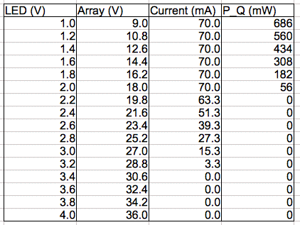
Transistor Q16 is ZXTP2025F in an SOT-23 package. According to its data sheet, this transistor should be able to handle 1000 mW continuously while mounted on a circuit board with ground plane. Our Luxeon Z blue LEDs have forward voltage drop around 2.8 V, and we find we deliver 34 mA with the A2082A. Our Luxeon Z deep red LEDs have drop closer to 1.8 V, and so will receive 70 mA in a nine-LED array while Q16 dissipates 200 mW.
[25-MAR-15] Our main radiation test page is here.We have A2082X number X1 that has received 1.4 kGy of cesium-137 gamma rays. Its +5 V quiescent current rises by has risen from 3 mA to 12 mA. The 3V5 power supply is at 3.6 V, which is the same as before irradiation, and the 1V8 supply is at 2V0, also the same as before. When we wake up the board, we get 92 mA from +15 V, 13 mA from +5 V, and 84 mA from −15 V. Much of this current consumption is due to saturation of the thermometer amplifier, and our original lower value for R26. But the current consumption of the analog switch and the op-amps appears to be typical for un-irradiated circuits. We capture this image with a new sensor. We scan the board with a programming cable and erase the existing program, but we cannot re-program the board. The logic chip, U4, has no valid firmware and the board no longer works.
[31-MAR-15] We heat up U4 on X1. We freeze U4. We put 5 kΩ from TCK to 0V. We put 5 kΩ from TDO to 1V8. The device still won't program.
[02-APR-15] We note that the ICX424 vertical clocks can tolerate −15 V. Our A2082X applies 0 V and −7.7 V, as recommended by the data sheet. After ionizing radiation, we expect positive charge to be trapped in the device's gate oxide. If so, we must apply a lower voltage to the vertical clock phases if we are to set up the potential fields required for proper operation of the transfer area pixels.
We have an ICX424AL that has endured 475 Gy, see here. We connect it to our A2082X. We decrease the low-level voltage of the vertical clock phases V1C, V2C, V3C, and the bias voltage VL, from −7.7 V to −10 V by loading 33 kΩ in parallel with the 10 kΩ resistors loaded for R50, R54, R57, and R59. We drop the low-level voltages to −12.5 V by putting another 33 kΩ resistor in parallel with each. The following table shows the transfer area dark current in counts per row that we obtain with the Dosimeter Instrument, and also a link to an image we took with single-pixel readout and 10-ms exposure in ambient light.
| Clock Level (V) |
Image at 475 Gy |
Dark Current at 475 Gy (counts/row) |
Dark Current at 0 Gy |
Image at 0 Gy |
|---|---|---|---|---|
| −7.7 | Saturated | 0.283 | 0.000 | Sharp Contrast |
| −10.0 | Sharp Contrast | 0.111 | 0.000 | Sharp Contrast |
| −12.5 | Sharp Contrast | 0.118 | 0.000 | Sharp Contrast |
The −10 V clock level appears to decrease the transfer area dark current by a factor of 2.5. Assuming no other failure occurs in the IXC424 at higher doses, this factor of 2.5 increases our ionizing radiation tolerance from around 500 Gy to 1.2 kGy.
[06-APR-15] We try two 500-Gy sensors, No1 and No2 and we vary V1-V3 separately from VL. Our −10 V levels for all four signals is still the best.
| V1-V3 (V) |
VL | Dark Current 500 Gy No1 (counts/row) |
Dark Current 500 Gy No2 (counts/row) |
|---|---|---|---|
| −7.7 | −7.7 | 0.116 | 0.096 |
| −10.0 | −10.0 | 0.040 | 0.037 |
| −10.0 | −12.5 | 0.044 | 0.040 |
| −10 | −7.7 | No Image | No Image |
[06-MAY-15] We have an A2082A that has received 1.6 kGy in our cesium-137 gamma-ray source. It captures images from four image sensors. It flashes all LEDs. The thermometer readout is broken. When we select T1 with no RTD attached, K+ is at 380 mV. We obsere failure of the temperature measurements at 330 Gy in our experiment. We remove R18 and R21 and K+ goes to 14.4 V. It turns out that the P2082A02 firmware applies 3.5-V bias to the gates of Q9 and Q15 when the device is asleep. These mosfets are damaged. We replace them and the temperature readout with the five remaining mosfets, all of which received 1.6 kGy without gate biase, is accurate and precise.
The P2082A02 firmware makes sure all mosfet gates are at 0V when the device is asleep, as was the case in our first irradiation, in which the RTD readout worked after 1.4 kGy. We take images like this from four ICX424 image sensors that have received 1.4 kGy. Our image sensor readout, RTD readout, and LED flashing all appear to work well enough up to 1.4 kGy.
[27-MAY-15] We measure the threshold voltage of various NDS355AN mosfets. Two that had 3.5-V gate biase and 1.6 kGy have threshold −2.0 V and −2.8 V. Five that had 0-V bias and 1.4 kGy have threshold 0.4 V. Four new mosfets had threshold 1.6 V. The unbiased damage rate appears to be −0.86 V/kGy. In an earlier experiment we found the damage rate to be −0.9 V/kGy.
[19-JUN-15] We have two A2082As, No5 and No6, and four LC4128ZC chips back from a 20-Tn neutron irradiation. Neither of the A2028s will loop back. The LM4050 voltage references are damaged. We remove them, connect them to +15V through 22 kΩ, and measure the voltage across them. We compare them to fresh samples. The 4.1-V device gives 4.2 V when fresh and 4.7 V after 20 Tn. The 2.5-V device gives 2.6 V when fresh, 2.8 V after 20 Tn. We replace the damaged voltage references on No5 and the logic chip outputs oscillate. The 1V8 power supply oscillates also, at the same frequency, between 1.0 and 1.3 V. We cannot re-program the logic chip, but the 1V8 power supply does stabilize at 2.0 V during our re-programming efforts. As soon as we power up again, 1V8 is once again oscillating around 1.1 V. Meanwhile, we load one of the irradiated logic chips onto an A208201B circuit board with all components from the first two pages of the schematic. We program it and take thermometer measurements. The logic chip is working perfectly.
[22-JUN-15] We replace R1=10kΩ with R1=2.2kΩ on No6. The lower resistor supplies more base current to Q1, the NPN transistor ZXTN2031F. The circuit powers up with 1V8 = 2.4 V and 3V5 = 4.4 V, as a result of the damaged voltage references. But neither of these voltages exceeds the absolute maximum ratings for the U4=LC4128ZE logic chip or U1=SN65LVDM180D transceiver. We take sharp images with an ICX424AL. We speculate that the current gain of Q1 dropped to the point where it could not supply the turn-on current demanded by U4. The damage to the voltage references appears to be non-fatal for the image capture.
[25-JUN-15] The No6 irradiated circuit consumes 0.5 μA from +15V and 0.0 μA from −15 V when asleep, 50 mA from +15 V and 42 mA from −15 V when awake. It flashes LEDs and reads temperature. It takes images. It appears that the NPN and PNP transistors, although damaged, are still sufficiently functional to switch power and current.
[30-JUN-15] As we report elsewhere, we measure the drop in gate threshold voltage of the NDS355AN and find that our thermometer selector should be tolerant of at least 2 kGy, provided we make sure we do not apply gate bias to the transistors when the board is asleep.
[28-APR-16] We subject an A2082A to 15 Tn of fast neutrons at the UMass Lowell reactor. Afterward, its connectors are active and we leave it in a draw for a few days. We capture images and flash LEDs. The board behaves normally.
Note: All our schematics and Gerber files are distributed under the GNU General Public License.
S2082_1: LWDAQ Interface.[10-FEB-15] Printed circuit board A208201A submitted for fabrication.
[24-FEB-15] We are able to program the logic chip. We adapt the H-BCAM firmware to make A2082A01.abl. Logic bits respond. Loop-back works.
[26-FEB-15] The wake/sleep switch as it is now, does not work. The origina, flawed, circuit we present below.
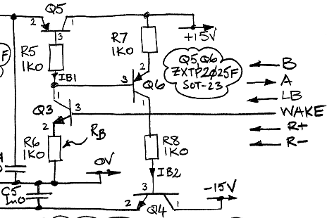
The emitter of Q6 is connected to +15V through R7. On !WAKE, Q5 turns off, which should take +15V down to 0V, but in that case the base-emitter voltage on Q6 becomes 15V, and breakdown of the base-emitter junction occurs at around 8 V for the ZXTP2025F. Thus Q6 starts to conduct to 0V, which turns on Q5, raising +15V up to 7 V, where the base-emitter breakdown reaches equilibrium with the Q5 base current. We connect R7 to J1-7 and the switch works perfectly. The new switch is shown in the updated schematic.
We load all remaining components. We measure VCOM = 1.37 V. Quiescent current with the board asleep is 0.5 mA from +15V, 3.6 mA from +5V and 0.0 mA from −15V. We load all remaining components. Quiescent current with board awake is 51 mA from +15V, 5.0 mA from +5V, and 41 mA from −15V.
Our 390 Ω resistors turned out to be 390 kΩ. We replace them all with 330 Ω. We get the following image with ICX424Q quadruple-pixel readout.

The gain of the A2082X is set so that the quadruple-pixel saturation occurs just below intensity 255 in the digitized image. Here, the saturation level is a little above 255 because we have 330 Ω resistors in the output divider (R70 and R86 here). The saturation level for single-pixel readout, meanwhile, is at around 117.
[31-MAR-15] We have firmware P2082A02.abl. We modify the Thermometer Instrument to read out the four temperature sensors and top and bottom reference resistors of the A2082. Thermometer readout with some test RTDs is accurate to ±0.1°C in a room temperature water bath. Dynamic range is −10°C to +27°C.
[03-APR-15] In P2082A02.abl, we increase the length of the HI pulse on the horizontal clock, H, from 7 to 12 HCK periods. The commercial-grade 7.5-ns device has HCK period roughly 15 ns, so we now have the pixel value being asserted for 180 ns instead of 105 ns. We assert R for two clock periods immediately after H goes LO. In quadruple-pixel readout, we now allow two HCK periods for the initial HI and LO pulses, which greatly eases the demands on the clock drivers.
After changing the pull-up and pull-down resistors on our A2071E driver from 10 kΩ to 1 kΩ, we are able to capture images at the end of a 120-m root cable, both with quadruple- and single-pixel readout.
[06-APR-15] We have two prototype extension arms. Because of an error in the schematic, J1 has its pins reversed, so we turn it around and connect from the other direction. We are able to capture single- and quadruple-pixel images from all four images at the end of a 12-m cable by selecting device ID 1-4. The photograph below shows the quadruple-pixel horizontal clock signals with four ICX424s loading the level-shifting op-amps.
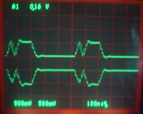
We obtain these clock signals, as well as a clean reset pulse, with the digital signals passing through 100 Ω on their way to the op-amp, which introduces a time constant of 10 ns, then with 15 pF across 1 kΩ in the feedback path of the level-shifter, for another time constant of 15 ns, and finally a 10-Ω series resistor at the level shifter output (see schematic)
[08-APR-15] With R27, R10, and R11 = 2.0 kΩ, the dynamic range of our temperature measurement is −10°C to +27°C. The center of the range should be 20°C. We observe that Q5-1 cannot go more than one diode drop below VCOM because of the parasitic diode across the transistor. We increase R7 to 10 kΩ, thus reducing the gain of U5-7 from 6.0 to 2.0. Now we get range −22°C to +50°C.
[14-APR-15] We replace R70 and R86 with 100 Ω (were 390 Ω) so as to increase the gain of the video amplifier. Saturation now begins at about 230 counts with a short cable and single-pixel readout. We change R66 and R67 from 390 Ω to 1 kΩ. Thermometer dynamic range is now −20°C to +48°C.
[25-APR-15] We change R1 to 2.2 kΩ on the schematic and in the bill of materials.
[13-AUG-15] When we touch the via next to the base of Q6, the −15 V power supply turns on to around −5 V. When we remove our finger, it stays at −5 V for servaral minutes, or in some cases for days. We clean thoroughly and bake dry. All such boards now perform better. We apply an acrylic coating to Q6 and surroundings. When the coating is cured, we touch Q6 and get −5 V on the −15 V supply, but the supply goes back to 0 V as soon as we remove our finger. We resolve to make sure the boards are as clean as we can get them, then apply acrylic coating to Q6.
We find that our A2082A reading out the same RTD at room temperature gives measurements up to 0.3 °C different from an A2053A. The latter circuit is well-proven, so we suspect a problem with the A2082A. We note that the resistance in series with the collector of Q8 should be 1080 Ω, but in our original schematic is 1037 Ω We replace R16 with 330 Ω.
We note that the A208201B circuit board does not connect the four mounting holes to the shield of the LWDAQ branch cable. The shield is connected only to 0V on the circuit board through a 10-nF capacitor. But this hardly matters because the cable running to the A2082A inside a nSW alignment bar has no shield. The shield ends when the cable get to the entrance to the bar.
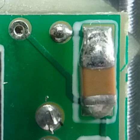
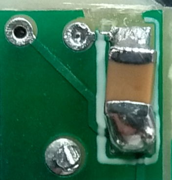
[13-MAR-19] We have Bar 5 A-side not taking images and Bar 15 C-side taking neither images nor temperature measurments. They behave as if one of the image sensor clock phases is shorted to the alignment bar in Bar 5 and +15 is shorted to the alignment bar in Bar 15. We discover another problematic bar pre-installation at Freiburg University. We trace the short to a +15V via on one of the image sensor heads
