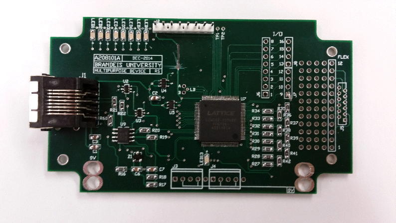
Figure: A208101B Multi-Purpose Device. BNC connectors omitted.
| Default Firmware |
| Code |
| A208101A |
| VHDL |
| A208102A | A208002A |
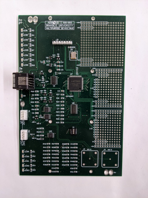
The A2081 is a multi-purpose device that controls analog and digital inputs and outputs with a LCMX02-1200ZE programmable logic device by Lattice semiconductor. The A2081 combines elements of the A2057 input/output head and the A2060 programmable logic head (which we often use in tandem) on one board.
The A2081 contains two analog inputs which can read the 16-bit ADC of the A2071 via the Voltmeter instrument. Two buffered analog outputs (0-3.3V) are controlled directly by the logic pins of the LCMX02-1200ZE. A future version of the A2081 will contain gain resistors that allow the range of the analog output to be set manually.
Twenty-five digital logic input/output pins are provided on the A208101A. Sixteen are routed to standard inline package (SIP-4/SIP-8) footprints and nine are routed to footprints for P0805 LEDs. Behavior of the input/output pins is determined by the firmware of individual devices. The default firmware for the A2081 contains an opcode which sets either the upper or lower bytes of the I/O or the single byte of eight LEDs. The red "error" LED is not used by the default firmware.
The A2081 receives commands as defined by the LWDAQ specification.
| DC16 | DC15 | DC14 | DC13 | DC12 | DC11 | DC10 | DC9 | DC8 | DC7 | DC6 | DC5 | DC4 | DC3 | DC2 | DC1 |
|---|---|---|---|---|---|---|---|---|---|---|---|---|---|---|---|
| D7 | D6 | D5 | D4 | D3 | D2 | D1 | D0 | WAKE | LB | SEL1 | SEL0 | OP3 | OP2 | OP1 | OP0 |
The default firmware for the A2081 uses a four bit operation code and a two bit selector. Data bits and selector bits determine board behavoirs depending on the operation code.
| Operation | Opcode | Hex Code | Selector |
|---|---|---|---|
| Output Reset | 0000 | 0 | N |
| RAM Single Command Upload | 0100 | 4 | N |
| RAM Output Period Select | 0101 | 5 | Y |
| Select RAM DAC Output | 0110 | 6 | Y |
| Analog Input | 1000 | 8 | Y |
| Analog Output | 1001 | 9 | Y |
| Digital Output | 1011 | B | Y |
| Board Test | 1111 | F | N/A |
Board Reset sets all outputs to 0. RAM Output to DACs is halted. RAM address is reset to 0. RAM write flag is de-asserted. Analog return is allowed to float.
The default A2081 is set up to store 512 commands for DAC output in the on-chip "Embedded Block RAM" of the MachXO2-1200ZE. Send a command "0000" to assert that the address of the first byte is 0. Sending a command with the opcode "0100" will set the value of that byte to the eight bit value of DC16-DC9, with DC16 as the most significant bit. (Ex.: FF84 will set the byte to 255.) Send 512 consecutive commands to the board to record a complete signal.
The default A2081 firmware stores a 24-bit value representing the number of delay ticks on automatic DAC output. Sending a command word with the opcode "0101" will set the number of delay ticks in the RAM countdown timer to the value of DC16-DC9. The use of the selector bits determines whether bits 23-16, 15-8, or 7-0 will be set. For example, if the timer is set to zero, sending FF85 will set the timer to 255 ticks of 50 ns each. Subsequently sending FF95 will set the timer to 65536 delay ticks. The DAC output byte address is incremented each time the countdown timer reaches zero.
The default A2081 will output the values stored in the RAM (by use of opcode 0100) at the selected frequency (by use of opcode 0101). Use the selector bits to establish output to DAC "A" (S=01), DAC "B" (S=10), or both (S=11). Sending 0110 with selector bits 00 will set both DACs to 0.
Establish analog return to the driver from one of four nodes by sending opcode 1000 to the A2081. The principal purpose of this is for use with the driver's adc_16 job. Selector bits DC6 and DC5 determine the channel to be measured.
| Selector Value | Analog Return |
| 00 | 0V Reference |
| 01 | ADC "1" |
| 10 | ADC "2" |
| 11 | 5V Reference |
Altering this behavior for special versions of the A2081 firmware is not recommended as this functionality is used by the Voltmeter instrument.
Asserts control of the DAC. If the RAM-driven signal generator output is active, command "1001" will stop it. Data bits DC16-DC9 set the eight-bit DAC value. Selector bits DC6 and DC5 determine which DAC will have its outputs updated. Unlike the signal generator, opcode "1001" supports two different DAC levels.
| Selector Value | I/O Bank |
| 00 | Output = 0V |
| 01 | DACA |
| 10 | DACB |
| 11 | Both |
Digital Input is not yet implemented. Future versions of the A2081 will support using any of the 16 IO pins as digital inputs. The state machine of the P2081B accomplishes this by disabling digital output on IO9-IO16.
Voltage at the 16 I/O pins can be set to 0 or 3.3V by use of command word "1011". The value of DC16-DC9 will replace the entire byte. The bank of 8 indicator LEDs can also be turned on or off. Selector code 00 sets all logic and LED outputs to 0.
| Selector Value | I/O Bank |
| 00 | Output reset |
| 01 | IO8-IO1 |
| 10 | IO16-IO9 |
| 11 | LED8-LED1 |
Opcode "F" is reserved for use as a board test. It is our habit to send "FFFF" to a device when we want to verify that commands are being received. We're not good at breaking habits, so we reserve this word. The board displays its firmware version on the eight green "data" LEDs.
Note: All our schematics and Gerber files are distributed under the GNU General Public License.
S2081_1: LWDAQ Interface, Schematic Page One| Firmware Version | LED Code | Purpose | Notes |
| A | 00000001 | General IO | |
| B | 00000010 | X-Ray Control Circuit | Does Not Respect Wake Bit |
| C | 00000011 | LED Pulser Circuit | Limits ADC Frequency. Logic I/O Bypassed. |
| Version | Firmware | Extension Circuit Diagram | Description |
|---|---|---|---|
| Default | A | None | Preinstalled 2081 Functions |
| X-Ray Controller | B | S2081B | Controls for 50kV Power Supply via DAC and IO |
| LED Fast Pulser | C | S2081C | 25 ns Pulser for Driving LEDs |
Development notes relevant only to obsolete versions of the A2081 Multi-Purpose Device have been archived using HTML comments.
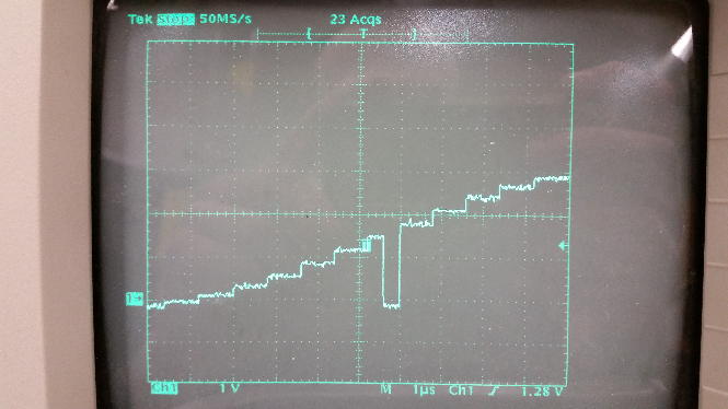
[11-FEB-2015] We build the analog to digital converters with 1% 2K resistors and 5% 1K resistors, because that is what we have on hand. We obtain the following outputs with a A2057 Voltmeter and a LWDAQ tool script:
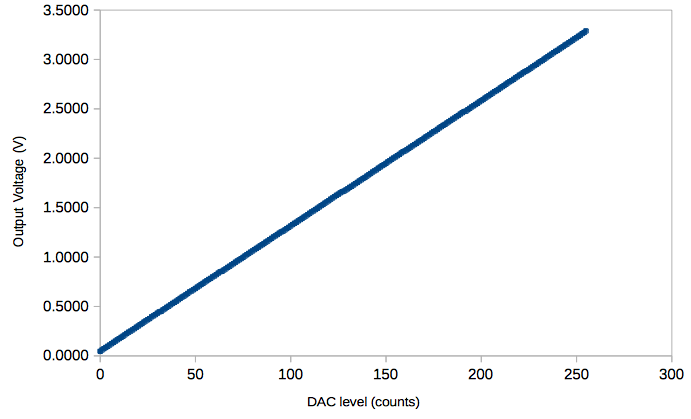
We expect to see an increase from 0 to 3.3 volts in increments of 12.9 mV per bit. We observe rather that the DAC increases from ~46 mV to 3.28 with increments of 12.7 mV per bit. We observe the 46 mV floor when we measure ground with the oscilloscope probe, even when we touch the scope probe to its own ground.
This offset is reduced with each additional resistor. The following graph shows the residuals when the data is compared to ideal DAC behavior:
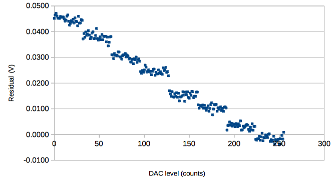
The residuals change sharply when a new bit is added to the output. We will order 1% accurate 1k resistors and try again.
[13-FEB-2015] We observe that the DAC output value falls between signals. The state machine is interpreting address words as command words. We write a LWDAQ tool script to send sequences of command and address words to the device.
[end-FEB-2015] We create a single-process VHDL state machine to control the command receiver. We correct the code recording the initial bit of the transmitted word to properly handle address words.
[25-MAR-2015] The opcode for analog output is set to "1001". Both DACs respond properly to command words.
The Opcode for analog return to the driver is set in firmware to "1000". We alter the Voltmeter instrument to send commands to the A2081. The top and bottom reference voltages properly read 0V and 5V when we set the Voltmeter analysis_auto_calib to 1 and the device elements to 3 and 4 respectively. We realize we designed the board for the DG412, not the DG411, and invert the logic signals in the firmware. This will cause a few microamps to flow from 15V on commands like "0080", but does not otherwise affect the board.
We note that the Voltmeter will return a 5V signal for any steady voltage on the 5V reference. We remove device element "3" and "4" from the Voltmeter.
When we put a voltage across the terminals with our bench power supply we get an accurate reading. However, the channels do not read 0V when they have no signal, but rather 1.35V. We put 1 megaohm between ADC1 and ground and it reads 1.27V. We replace that with 1 kiloohm and it reads 51 mV. We try 50 ohms and it reads 1.6 mV. It seems the input impedance of the channels is too low, so we will have to redesign the circuit. The A2057 avoids this problem by having buffer amplifiers on its inputs.
[08-APR-2015] We see a 0.2 volt output on the DAC when the board is asleep. We remove an error in the firmware that connected all four switches when the sleep command is sent. With the switches properly open, this output jumps to 0.7 volts. We watch the output of the DAC on "wake" and see the following waveform:
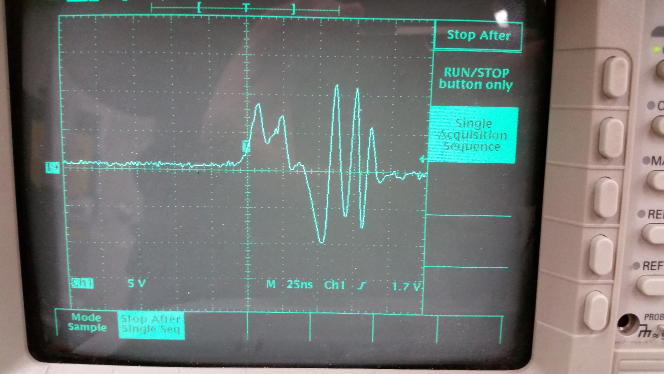
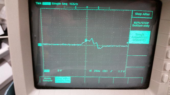
There is no unexpected activity on the DAC logic outputs of the logic chip. They remain at 0V during both wake and sleep transitions.
[09-APR-2015] We complete a first version of a function generator using the RAM and DACs of the 2081. We program it to send a sine wave and get the following result:
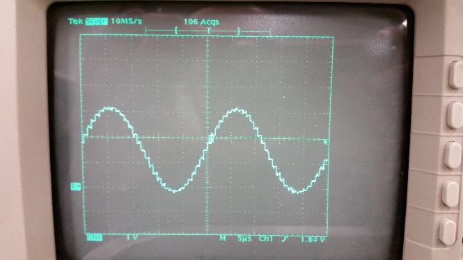
We observe that there is an occasional drop to 0 between cycles of the sinewave output. It only occurs between cycles and never during the cycle. We randomly stop the digital oscilloscope readout at the appropriate point 16 times and observe the behavior once. The output stays at zero for one "divided clock" cycle; in this case 400 ns.
Some change in the firmware unexpectedly made the command strobe 50 ns long, rather than 25 ns long. This caused command words to be executed twice in certain situations. We change the behavior of the command receiver so that the state updates on the falling edge of the 40MHz clock. This corrects the problem. Since correcting the "double command" issue we have not seen the intermittent failure in the DAC output.
We change the command receiver process so that there is a wait until CLK = "1" rather than several if rising_edge(CLK) statements. The Synplify synthesis tool now creates the state machine with one state register instead of two, shortening command strobe to 25 ns. We change back to if rising_edge(CLK) but only use one large if statement, and command_strobe remains 25 ns.
[09-JUN-2015] The DG411 is an active-low switch, so when the board is asleep we send a 3.3V logical HI to each of the ADC control inputs. However, the DG411 also contains diodes that clamp all inputs to V+ and V-. When the board is asleep, V+ and V- are at 0V, and will conduct current. We believe up to 30 mA is flowing through each of the channels from the logic chip to ground. This is likely limited by the maximum output current of each pin of the logic chip. To correct this, we replace the DG411 with the DG412, which has active-high switches.
[21-SEPT-2015] We have been using the A2081B, which makes several improvements on the A2081A.Various circuit boards have been printed specifically for use with the A2081. We keep an archive of their use here.
The A208102A is an array of variable size that connects switched P0603 LEDs (up to 8 in series) to the Multi-Purpose Device's patch area. It requires connection to +15V, -15V, Logic, and Ground.
S208102_1:Switched LED ArrayThe A208002A is an array of Luxeon-Z LEDs that connects to the A2081 patch area. It was used in testing the ferrule placement for the A2080 contact injector. It has an on-board
S208002A: LED Array for Contact Injector Prototype.