ADC Tester (A2100)
© 2007-2008, Kevan Hashemi
Brandeis University HEP
Contents
Introduction
Design
Specification
Memory
Instructions
Current Measurement
Sample Sessions
Sampler Tool
Regulator Stability
Results
Introduction
The ADC Tester (A2100) is a LWDAQ device that records the output and power consumption of two ADCs. Its original purpose was comparative testing of two ADCs at different temperatures, but it turned out that the A2100 makes a good dual-channel eighteen-bit oscilloscope.

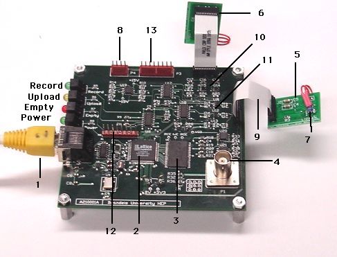
Figure: ADC Tester (A2100A) with Two LTC1865L Auxilliary Boards. The flex cables are short for the benefit of the photograph. We give the names of the four indicator LEDs. (1) RJ-45 connection to LWDAQ, (2) programmable logic chip, (3) 512K×8 static RAM, (4) Analog signal input, (5) ADC1 auxilliary board, (6) ADC2 auxilliary board, (7) Pt 1000 RTD glued to LTC1865L, (8) connection for two additional RTDs, (9) 12-way flex cable, (10) fixed voltage supplies for ADC2, (11) fixed voltage supplies for ADC1, (12) logic programming connector, (13) connection to Resistive Sensor Head (A2053L).
The two ADCs do not reside upon the A2100. They reside on auxilliary boards, which are separate, miniature circuit boards connected to the A2100 by 12-way, 1-mm pitch, 25-cm long flex cables. In a sampling session, the A2100 takes simultaneous, regular samples from both ADCs and stores them in its 512 KByte memory. Once the sampling session is over, we can read out some or all of the samples and analyze them.

Figure: LTC1865 Auxilliary Board. (1) LTC1865 sixteen-bit 250-kHz ADC in MSOP-10 package, (2) 1000-Ω RTD fastened to top side of ADC with super-glue.
We control and read out the A2100 with our LWDAQ Software. We use the program's Terminal Instrument to define sampling sessions and read out blocks of ADC samples. We use the Gauge Instrument to measure the currents supplied through the fixed voltages.
Note: We designed the A2100 to compare the response of two ADCs at different temperatures when presented with the same input. In particular, we wanted to study the performance of the AD7982 at −140°C. The AD7982 is an 18-bit, 1 MSPS, serial-interface, differential-input ADC in an MSOP-10 package. In case the AD7982 failed at low temperatures, our hope was that the A2100 combined with new auxilliary boards would allow us to test other ADCs as well, one of which might work at low temperatures. We produced three auxilliary heads for these ADC tests: one each for the AD7982, LTC1865, and AD7980.
The A2100 provides the following.
- One BNC plug for 50-Ω input from function generator.
- Same fully-differential input to both auxilliary boards.
- Noise on ADC common-mode input voltage with BNC input grounded <8 nV/√Hz.
- Noise on ADC differential input with BNC input grounded <8 nV/√Hz.
- Four bi-directional logic lines to each auxilliary board.
- Simultaneous, periodic sampling and recording of ADC samples.
- Three stable, fixed 30-mA supplies to each auxilliary board.
- Measurement of current drawn from each fixed voltage.
- Resistive sensor connection to each auxilliaray head.
- Fixed voltages may be turned off as a group.
The resistive sensor connections allow us to put one resistive sensor on each auxilliary head. We use 1000-Ω platinum RTDs to measure the temperature of the auxilliary heads. The ones we used in these experiments were all purchased from Enercorp. The sensor elements are a thin film of platinum deposited on a ceramic base. The element's steel wires are soldered to teflon-insulated leads. (The teflon-insulated leads were part of a custom order from Enercorp.)
We will need to know the temperature of the auxilliary boards to ±5°C from −140°C to 30°C. We will not include resistance-measuring electronics on the A2100. Instead, we will connect the RTDs to a Low-Temperature Head (A2053L) by means of a separate connector on the A2100.

Figure: ADC Tester (A2100A) with Auxilliary Boards and Low-Temperature Head (A2053L). When we took the picture, we had just cooled ADC2 by immersion in liquid nitrogen, and now the ADC is warming up as it sits above the surface of the liquid. (1) Liquid nitrogen, (2) ADC2 above the liquid, (3) flex cable, (4) ADC1 at room temperature, (5) input from function generator, (6) LWDAQ connection for A2100, (7) RTD cable, (8) LWDAQ connection for A2053L, (9) the Low-Temperature Head (A2053L).
The Probe Auxilliary Board uses a THS4130 differential amplifier to provide a single-ended or differential input for an AD7982 eighteen-bit ADC. The board allows us to test the eighteen-bit settling time of the THS4130 after it comes out of its power-down mode. In the future, the Probe Auxilliary Board allows the A2100 to act as a dual-channel eighteen-bit oscilloscope.
Design
The A2100's LWDAQ interface and data memory are based upon those of the Data Recorder (A3007) designed by Open Source Instruments. The A2100 is simler than the A3007 in that it does not implement a RAM FIFO, nor does it allow simultaneous storing and retrieval of data.
S2100_1: First page of circuit diagram showing RJ-45 connection to the LWDAQ, programmable logic chip, reference oscillator, clock oscillator, and 512-KB static RAM.
S2100_2: Second page of circuit diagram showing more logic, indicator lamps, connections to auxilliary boards, analog input plug, and RTD connections.
S2100_3: Third page of circuit diagram showing fixed voltage supplies.
S2100_4: Fourth page of circuit diagram showing current measurement multiplexer, analog return to LWDAQ driver, common-mode voltages.
S2100_5: Auxilliary board for AD7982 with fully-differential input in MSOP-10 package.
S2100_6: Auxilliary board for LTC1865L with fully-differential input in MSOP-10 package. Switch reference and analog supplies to 5V for the slightly faster LTC1865.
S2100_7: Auxilliary board for AD7980 with pseudo-differential input in MSOP-10 package.
S2100_8: Probe Auxilliary Board for THS4130 and AD7982, creates an eighteen-bit 1-MSPS oscilloscope input.
P2100A07: Logic firmware in the form of an ABLE text file, for use with all auxilliary boards.
Specification
The A2100 conforms to the LWDAQ Specification in every respect except that of current consumption. It is LWDAQ Device Type 3 (DATA). It implements no element numbers. We give its command bit allocation below.
| DC16 | DC15 | DC14 | DC13 | DC12 | DC11 |
DC10 | DC9 | DC8 | DC7 | DC6 | DC5 |
DC4 | DC3 | DC2 | DC1 |
|---|
| I7 | I6 | I5 | I4 | I3 | I2 |
I1 | I0 | WAKE | LB | DRX | DTX |
X | X | X | X |
Table 1: Command Bit Allocation on the A2100.
The LB bit enables the logic signal return from the device and inhibits the analog return. The analog return is used to monitor the current supplied by the auxilliary board fixed voltages.
The DTX bit enables byte transfer from the device to the driver. The driver will provoke transmission of each byte by sending a stop bit. When the device receives the stop bit, it waits until its current sampling session comes to an end, and transmits the first byte of the sample data. Subsequent stop bits from the driver cause the transfer of subsequent bytes. If the device is not currently sampling, it transmits the byte immediately after receiving the stop bit.
The DRX bit causes the top eight command bits to be used as an instruction. Bits I0 to I7 form an eight-bit instruction. The A2100 will executes instructions immediately after it receives a command word with DRX set to one (see below).
The A2100 current consumption, as recorded by the Diagnostic Instrument when the device is both asleep and awake, is as follows.
| State | +15 V | -15 V | +5 V |
| Asleep | 6 mA | 6 mA | 43 mA |
| Awake | 6 mA | 6 mA | 43 mA |
Table: Current Consumption.
The LWDAQ limits are 5 mA from each supply when asleep, 200 mA from ±15V when awake, and 20 mA from +5V when awake.
Memory
The A2100 memory is a 512K × 8 static RAM. The RAM chip is U6 in the schematic, a CY7C1049CV33 from Cypress. Each time the A2100 takes a sample, it stores eight bytes in its memory, as shown in the following table.
| Byte | Contents |
|---|
| 0 | Value 1, indicates ADC1 |
| 1 | ADC1 Most Significant Byte |
| 2 | ADC1 Middle Byte |
| 3 | ADC1 Least Significant Byte |
| 4 | Value 2, indicates ADC2 |
| 5 | ADC2 Most Significant Byte |
| 6 | ADC2 Middle Byte |
| 7 | ADC2 Least Significant Byte |
Table: Contents of an Eight-Byte Sample.
As you can see from the table, byte ordering is big-endian. Each ADC accounts for four bytes. One byte is the ADC number. The other three bytes are the ADC sample. We use one byte for the ADC number so that later permutations of this circuit can have more than two ADCs but use the same data acquisition software.
The A2100 reads from and writes to the RAM location pointed to by its nineteen-bit data address. Each time it stores a byte, it increments the data address. Each time it reads out a byte, it increments the data address. At the end of a sample session, the A2100 resets its data address to zero. The A2100 does not support simultaneous reading and writing of data. During a sample session, the RAM is monopolised by data storage. At the end of the sample session, the bytes are available for download by the driver.
Instructions
The top eight bits of a command word act as an instruction if and only if the command word's DRX (or DC6) bit is set. Instructions contain an operation and an argument. Both are four bits long. The operations and arguments have the following meanings.
Instruction
(Hex) |
Operation
(Hex) |
Argument
(Hex) |
Function |
| 0x | NOP | x | No Operation |
| 1x | SSS | x | Start Sample Session |
| 2a | SFV | a | Switch Fixed Voltages On (a0) or Off (a=0) |
| 3n | CMC | n | Set Current Measurement Channel n |
| 4n | SRC | n | Set Sample Rate Code n |
| 5n | NSC | n | Set Number of Samples Code n |
| Fx | RST | x | Reset |
Table 1: Instruction Set. An x means "don't care". Use "0" in place of x for forward compatibility. Future circuits will respect the above table for x=0.
An SSS operation starts a sample session. The sample session records a number of samples determined by the number of samples code at a rate determined by the sample rate code. We set these codes with the NSC and SRC operations.
The SFV operation switches on or off the fixed voltages that supply power to the auxilliary boards. On power-up, and after a RST operations, the fixed voltages are turned on. The SFV operation allows us to turn off the fixed voltages if required by our current measurement calibration.
The RST operation aborts the current sampling session, sets the data address to zero, sets the number of samples code to zero, sets the sample rate code to zero, sets the current measurement channel to zero, and turns on the fixed voltages.
The CMC operation sets the current measurement channel, which selects one of the eight current measurements provided by the A2100.
Current Measurement
The current measurement channel selects one of eight current measurement channels for analog return, as shown in the following table. We set the current measurement channel with the CMC operation. There are eight channels in all. Six provide measurement of the six currents delivered to the auxilliary boards (see schematic). Two provide top and bottom reference currents. An analog multiplexer selects the channel and amplifiers drive the analog measurement voltage onto R+ and R− (see schematic).
Current
Number
(Hex) | Channel
Name | Command
Word
(Hex) |
|---|
| 0 | VB | 30A0 |
| 1 | VT | 31A0 |
| 2 | VR1 | 32A0 |
| 3 | VA1 | 33A0 |
| 4 | VL1 | 34A0 |
| 5 | VR2 | 35A0 |
| 6 | VA2 | 36A0 |
| 7 | VL2 | 37A0 |
| 8-F | reserved | reserved |
Table: Current Measurement Channels Numbers and Names.
The table above gives us the sixteen-bit command word we must transmit to select each channel. This command word must have LB (or DC7) set to 0 so as to disable the device's logic return and permit its analog return to propagate back to the driver. The command word must have DRX (or DC6) set to 1 so that the A2100 will execute the instruction contained in I7..I0 (or DC16..DC9).
The VB channel returns the bottom reference current measurement, which will correspond to 0 mA or some other lower reference current chosen during assembly. Resistor R31 sets the bottom reference current. The VT channel is the top reference current, set by R29. The VR1, VA1, and VL1 channels monitor the current drawn by the voltages supplied to the first auxilliary board. The VR2, VA2, and VL2 channels do the same for the second auxilliary board.
We read out, analyze, and display the current measurement channels using the Gauge Instrument. We configure the Gauge Instrument to work with the A2100 by changing its gauge_commands string. We set this to the list of commands given in the table above. At the TCL console in our LWDAQ program, you could enter the following line.
set LWDAQ_config_Gauge(gauge_commands) "30A0 31A0 32A0 33A0 34A0 35A0 36A0 37A0"
We also set the Gauge's ref_top_y and ref_bottom_y parameters to match the top and bottom reference currents that flow through R29 and R31 respectively (see schematic). Because R29 and R31 are marked TBD (to be decided) on the schematic, you will have to look at your A2100 and determine their values. In both cases, the reference current is 15/R, where R is the actual value of the resistor. In this calculation, we ignore the value of the current-sensing series resistor, which is 47 Ω. With R29 = 10kΩ, set ref_top_y to 1.500 to indicate 1.500 mA. With R31 = 0Ω, set ref_bottom_y to 0 to indicate 0 mA.
The dynamic range of the current measurement is 50 mA. The regulators will start to over-heat if you draw more than 25 mA. We obtain our best results with the Gauge Instrument's display_s_per_div (shown as Scale s/div in window) set to 0.001. Current resolution is 1 μA. Accuracy over 0 mA to 25 mA is better than 0.5%.
Sample Sessions
The sample rate code determines the sample rate for the next sample session. We set the sample rate code with the SRC operation.
Sample
RateCode (Hex) | Sampling
Rate (kHz) | Instruction
(Hex) |
|---|
| 0 | 0 | 40 |
| 1 | 1 | 41 |
| 2 | 2 | 42 |
| 3 | 5 | 43 |
| 4 | 10 | 44 |
| 5 | 20 | 45 |
| 6 | 50 | 46 |
| 7 | 100 | 47 |
| 8 | 200 | 48 |
| 9 | 500 | 49 |
| A-F | reserved | reserved |
Table: Sample Rate Codes and Sample Rates
The number of samples code determines the number of samples in the next session. We set the number of samples code with the NSC operation.
Number
of Samples
Code (Hex) | Number of
Samples | Instruction
(Hex) |
|---|
| 0 | ∞ | 50 |
| 1 | 50 | 51 |
| 2 | 500 | 52 |
| 3 | 5000 | 53 |
| 4 | 50000 | 54 |
| 5-F | reserved | reserved |
Table: Number of Samples Code and Number of Samples.
We start a sample session with the SSS operation. If the number of samples code is zero, the sample session will continue until the A2100 receives an RST operation. Otherwise, the sample session will terminate when the required number of samples has been recorded in memory. As the A2100 records samples, it increments its data address. Each sample takes eight bytes, as shown above. At the end of a sample session, the A2100 resets its data address to zero, and is ready to upload its memory contents to the driver.
Note: The actual number of samples recorded by the A2100 is slightly higher than the number given in the table above. Instead of 50 samples, the A2100 records 64. Instead of 50000, it records 50176. The actual numbers simplify our binary logic. Our firmware is full of such simplifications because we like it to compile fast. The P2100A04.able code compiles in a five seconds.
To acquire a block of sample data from the A2100, we use the Terminal Instrument. We set tx_ascii, tx_decimal, and tx_file_name to empty strings. We use tx_hex for a list of instructions that will set up the sampling session. With tx_hex = "F0 44 53 10" the Terminal transmits four instructions to the A2100. The first resets the device, the second sets the sample rate to 10 kHz, the third sets the number of samples to 5000, and the fourth starts the sample session. The session will last for half a second, after which the samples will be available for download.
After the Terminal sends the set-up instructions, it sends command word "00D0", which instructs prepares the A2100 for byte transfer. Each byte transfer increments the A2100's data address by one. We set the Terminal's rx_size equal to the number of samples. In this case, we set rx_size to 5000. The Terminal downloads the samples as soon as the sample session ends. The samples will be available in the Terminal's data image. The name of this data image is given by the Terminal's memory_name parameter. You can extract the acquired samples into a TCL variable with a command like this:
set samples [lwdaq_data_manipulate $config(memory_name) read $config(rx_size) 0]
For more about instruments, data images, and instrument parameters see LWDAQ Instruments. For more on the routine we call in the above command, see lwdaq_data_manipulate. The "config" array we refer to is the Terminal's configuration array.
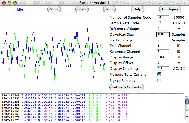
We control and read out the A2100 with our Sampler Tool. The figure below is a screen shot of the Sampler on MacOS. Download the tool script Sampler.tcl and run it with Run Tool from the LWDAQ Tool menu.

Figure: Sampler Tool. The two traces show the values obtained from two ADCs. In this case, the ADCs are AD7982s. The display range is 1 mV.
The Sampler output is a color-coded text line, as you can see in the screen shot.
Regulator Stability
With C1 and C2 (see schematic) both 10 μF, we saw a 1-V p-p, 100-kHz oscillation in +5V and 3.3V. The MAX6329 low drop-out regulator, U2, is oscillating. The oscillations affect the regulator's input and output voltages. We increased C1 and C2 to 20 μF by adding a second 10 μF capacitor in parallel. The oscillations stopped.
It occurred to us that the oscillations may have been caused by an excess of capacitance at the regulator input, or too high a ratio of capacitance to series resistance at the output. We tried the following combinations of capacitors and resistors and measured the oscillations for each combination.
| C1 | C2 | +5V Oscillation | +3.3V Oscillation |
|---|
| 20 μF | 20 μF | <10 mV | <10 mV |
| 10 μF | 10 μF | 1 V p-p, 100 kHz | 1 V p-p, 100 kHz |
| 10 μF + 10 Ω | 10 μF + 10 Ω | 1 V p-p, 100 kHz | 1 V p-p, 100 kHz |
| 10 μF + 2 Ω | 10 μF + 2 Ω | 200 mV p-p, 100 kHz | 200 mV p-p, 100 kHz |
| 10 μF + 1 Ω | 10 μF + 1 Ω | 100 mV p-p, 100 kHz | 100 mV p-p, 100 kHz |
| 10 μF + 0.5 Ω | 10 μF + 0.5 Ω | 600 mV p-p, 100 kHz | 50 mV p-p, 100 kHz |
| 10 μF + 1 Ω | 10 μF + 0.5 Ω | 600 mV p-p, 100 kHz | 50 mV p-p, 100 kHz |
| 1 μF | 10 μF + 0.5 Ω | <10 mV | <10 mV |
| 1 μF | 1 μF + 1 Ω | <10 mV | <10 mV |
| 1 μF | 1 μF Ω | <10 mV | <10 mV |
Table: C1 and C2 Combinations and Resulting Oscillations.
We see that 1 μF is better for both C1 and C2. No series resistor is required. But adding series resistance to a capacitor that is too large sometimes reduces the amplitude of oscillations..
Results
You will find our raw data in an Excel spreadsheet here. We presented the results of our ADC tests to the LSST Camera Electronics Group in January 2008. You will find our talk here.
LTC1865A
Note: We thought the devices we were working with was the 3.3-V LTC1865L. But they were in fact 5-V LTC1865As. The LTC1865A is specified to 250 kHz sampling rate and 20-MHz serial clock rate for supply range 4.75V to 5.25V and temperature 0°C to 70°C. When powered by 3.3V, the device works at 200 kHz from −180°C to 20°C.
[11-JAN-08] We begin with an LTC1865L auxilliary board, as shown here. We measured the current consumption of the LTC1865 at room temperature (20°C) and when immersed entirely in boiling liquid nitrogen (−196°C). We used the following Toolmaker script to obtain our graphs.
foreach {code rate} {41 1 42 2 43 5 44 10 45 20 \
    46 50 47 100 48 200 49 500} {
  set LWDAQ_config_Terminal(tx_hex) "F0 50 $code 10"
  LWDAQ_acquire Terminal
  set currents [LWDAQ_acquire Gauge]
  LWDAQ_print $t "$rate [expr 1000 * ([lindex $currents 4] - 0.057)]"
}
We obtained the following graph, which serves more to verify our firmware and software than to tell us about the performance of the LTC1865A. We are not recording the ADC samples yet, so we cannot be sure that the LTC1865A is functioning properly in liquid nitrogen. Furthermore, the LTC1865A is designed to operate only up to 250 kHz, so sampling at 500 kHz is unlikely to produce good data.

Figure: Current Consumption of LTC1865A, AD7982, and AD7980 with Sample Rate. The LTC1865A is powered by 3.3V instead of 5V.
[16-JAN-08] The A2100 is now fully-operational and we have Version 1 of the Sampler Tool. We plug two LTC1865L ADCs into the A2100. Both ADCs are configured to read IN− as a single-ended input.
Note: The serial clock speed we use on the A2100 to communicate with the ADCs is 20 MHz. The maximum clock speed recommended by the LTC1865A data sheet is 20 MHz. But we were operating the device at 3.3V, which is well below its recommended supply voltage of 5V. We found that we could transmit the code "1 1" to the ADC reliably, and so set it up for single-ended operation from IN−. But we could not transmit any other code reliably. Thus we used the LTC1865A only in its single-ended configuration for our initial tests.
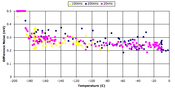
We record the standard deviation of the difference between the ADC1 and ADC2 samples at various sample rates as we cool ADC1 with liquid nitrogen or proximity to liquid nitrogen, and allow it to warm in the open air or above liquid nitrogen. We cool and warm the same chip over and over. It appears to suffer no damage. Nor does the RTD glued to its back come off or suffer any damage itself. The RTD always says −196°C when we immerse it in liquid nitrogen. We obtain the following graph, which shows the ADC functioning well all the way down to around −180°C. Below −180°C, if fails.

Figure: Difference Noise of LTC1865A with Temperature for Various Sample Rates. The ADCs are reading IN− as a single-ended input, and there is no signal applied to IN. We clip the difference noise to a maximum value of 0.5 mV so we can see the failure points at the top of the graph. The LTC1865A power supply is 3.3V instead of the recommended 5V.
We apply a 1-V p-p 5-kHz sine wave to the ADC inputs and measure the average and standard deviation of the difference as ADC2 cools down and warms up (previously we cooled ADC1, but we find the upside-down ADC2 orientation more convenient for cooling, as you can see in our apparatus photograph.

Figure: Affect of Temperature upon LTC1865A with 5-kHz, 1 V p-p Sine Wave Input. Sampling rate is 200 kHz. We measure current consumption from analog supply, the standard deviation of the difference between the cooled and room-temperature ADCs, and the average difference. Both ADCs convert IN− as a single-ended input.
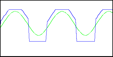
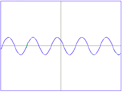
The LTC1865A consumes less than a microamp from its reference supply, even when it is running at 200 kHz, so its total current consumption is represented by its VA consumption. The figure below shows the failure that occurs below −190°C. The ADC still provides us with an output, but the output is distorted.

Figure: Failure of LTC1865A at −190°C. The blue trace is the output of the cooled ADC2. The green trace is the output of the room-temperature ADC1. The input is a 5-kHz 1 V p-p sine wave. The sample rate is 200 kHz.
The current consumption of the LTC1865A at 200 kHz and −180°C is less than 500 μA. We could use 2 LTC1865As in parallel to achieve a 500-kHz sampling rate with a total current consumption of less than 1 mA.
Note: The standard deviation of the difference between the two ADC outputs with no signal applied is around 250 μV. We are using a 3.3-V reference voltage, so this noise is 5 sixteen-bit ADC counts. If we assume the noise on each input adds in quadrature, our estimate of the noise on each input is 5/√2 = 3.5 counts.
[07-FEB-08] We discover that our LTC1865Ls are in fact LTC1865As. We raise VR and VA to 5V and try again to configure the chips to run with differential inputs. Below is a Sampler screen shot of the result.

Figure: Traces from Two LTC1865As with Differential Inputs. The input is a DC value. You can see the ADC count thresholds in the 100-point plot. The difference noise is around 140 μV. With the 5-V reference, one 16-bit ADC count is 76 μV.
The differential input configuration appears to be working well. The noise on the inputs drops from 600 μV with single-ended inputs to 150 μV with differential inputs. The difference noise remains roughly the same: 140 μV. But in terms of ADC counts, the difference noise has dropped: from 3 down to 2 counts. The noise generated independently by the ADCs must be less than 2/√2 = 1.4 counts.
AD7982
[25-JAN-08] The AD7982 needs a 2.5-V analog supply to run its internal circuits, a 3.3-V logic supply to match its serial interface with our 3.3-V logic, and a 5-V reference voltage for the best signal-to-noise performance at its input. We replace the 3.3-V regulators we used to provide VA for the LTC1865L with 2.5-V regulators. We add 3.3-V regulators for VL. For the moment, we leave the existing 3.3-V regulators in place for VR. We try the LTC1865L with these voltages, but it does not work. We know from past experience that the LTC1865L will work with VA as low as 2.4 V. The problem here must be that VR > VA, which is not recommended in the data sheet.
The AD7982s work immediately. We modify our Sampler code to handle the signed (twos complement) samples produced by the AD7982. The maximum positive output from the ADC corresponds to +VR, which is now +5 V. The maximum negative output is −5 V. The inputs are fully-differential.
At room temperature, the differential input noise on each ADC input is 230 μV and the difference noise is 140 μV, as shown in this screen shot. When we apply a ±0.5-V, 5-kHz sinusoid to IN with a DC offset so that IN+ is 2.5±0.5 V and IN− is 2.5±−0.5 V. The differential input voltage is therefore ±1 V.

Figure: Response of AD7982 to Sinusoidal Input. The input is ±1 V, 5-kHz, differential. The display range is ±5V, the number of samples displayed is 100. Sampling rate is 100 kHz.
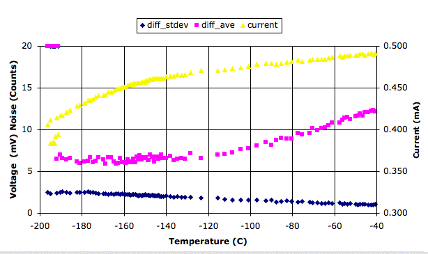
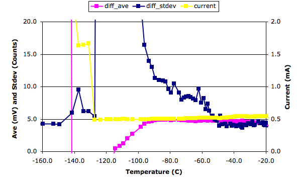
We remove the sinusoidal input and cool down ADC2. We obtain the following graphs with no input. The AD7982 is sampling at 200 kHz.

Figure: Affect of Temperature upon AD7982 with No Input. Sampling rate is 200 kHz. We plot total current consumption of the chip, the standard deviation of the difference between the cooled and room-temperature ADCs in 18-bit counts, and the average difference in mV. Both ADCs convert IN as a differential input. Raw data here.
The difference noise starts to rise sharply when we cool the ADC below −50°C. We get inversion of the average difference between the ADCs at −120°C. The current consumption jumps up sharply at −120°C. We obtained our measurements with two full cool-down and warm-up cycles, so the changes are consistent with temperature. We obtained almost identical results with two other AD7982s.
Detail: We were surprised at the failure of the AD7982 at −80°C. We went through our firmware and the AD7982 data sheet looking for possible errors on our part that may have cause the failure. We changed the phases and frequency of our serial clock. But we obtained the same results every time, or our changes broke the communication with the ADC. We are convinced, therefore, that we are driving the ADC correctly.
If we use only the top 16 bits out of the AD7982, we will reach 3 sixteen-bit counts of difference noise, which is roughly what we get from the LTC1865L, at −90°C. We conclude that the best we can hope for from the AD7982 is sixteen-bit performance at −90°C, but the device's performance degrades rapidly below −90°C.
We measured AD7982's current consumption at room temperature with sample rate using the following Toolmaker script.
foreach {src rate} {41 1 42 2 43 5 44 10 45 20 \
    46 50 47 100 48 200 49 500} {
  set Sampler_config(src) $src
  LWDAQ_print -nonewline $Sampler_info(text) "$rate " red
  Sampler_execute Acquire_Step
}
We added the results we obtaine to the graph above.
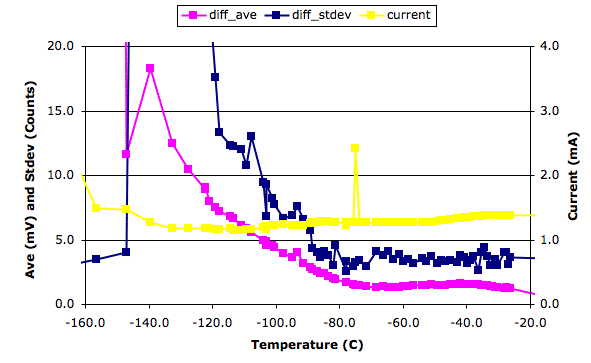
We repeated our cool-down and warm-up test with the AD7982 at sampling rate 500 kHz, and obtained the graph below. We cannot explain the spike in current at around −75°C. The spike may be a measurement error. We will repeat the experiment when we have a chance.

Figure: Affect of Temperature upon AD7982 with No Input. Sampling rate is 500 kHz. Raw data here.
AD7980
The AD7980 is pin-compatible with the AD7982, but its negative input is grounded internally. We connect IN+ to the ADC + input and 0V to the − input. The output of the AD7980 is unsigned, so the total range of the 16-bit samples is 0-5 V.
The AD7980 works immediately with our existing hardware and firmware. We obtain the following plot of current, average difference, and difference noise. The plot contains data we obtained during a cool-down and warm-up cycle.

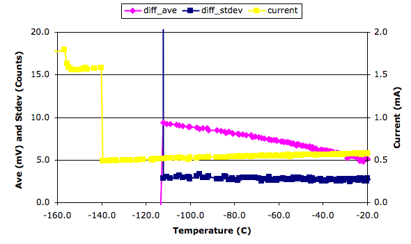
Figure: Affect of Temperature upon AD7980 with No Input. Sampling rate is 200 kHz. We plot total current consumption of the chip, the standard deviation of the difference between the cooled and room-temperature ADCs in 16-bit counts, and the average difference in mV. Raw data here.
The AD7980 failure is abrupt at −110°C. Above that temperature, its difference noise is like that of the LTC1865L: around three or four sixteen-bit ADC counts. You will find the current consumption of the AD7980 plotted verses sample rate at room temperature here
THS4130
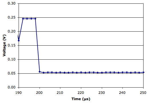
The THS4130 is a fully-differential amplifier. We use it in the Probe Auxilliary Board to turn a single-ended input on a BNC plug into a differential input for an AD7982 eighteen-bit ADC. on the Probe Auxilliary Board, the SDI logic signal connects to the THS4130 !PD (power down) pin. When HI, this pin enables the amplifier. We modified the A2100 firmware so that it enabled the THS4130 500 ns after sample number 99. We set the sample period to 2 μs and recorded the following graph with the Probe Auxilliary Board input open-circuit.

Figure: Settling of THS4130 after Enable. We enable the amplifier at time 198.5 μs. Sample period is 2 μs.
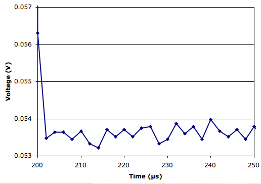
We enable the THS4130 at time 198.5 μs. Sample number 100, which takes place at time 200 μs, is slightly higher than the subsequent samples, as shown in the graph below.

Figure: Settling of THS4130 after Enable. We enable the amplifier at time 198.5 μs. Sample period is 2 μs.
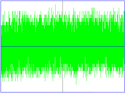
The following graph shows 5000 samples taken with period 1 ms, starting 1 ms after we enable the THS5130. The graph covers a 5-s period. The standard deviation of the voltage is 200 μV. The slope we obtain from this and repetitions of the same graph is less than 10 μV/s.

Figure: Settling of THS4130 after Enable. Shown are 5000 samples with period 1 ms. Full scale is ± 500 μV. One 18-bit count is 40 μV.
Because our input noise is 200 μV, we cannot measure the 40-μV (1 18-bit count) settling time of the THS4130. We can, however, measure the 160-μV (1 16-bit count) settling time. The 16-bit settling time is greater than 1.5 μs but less than 3.5 μs.
