ADC Cold Tests
Camera Electronics Workshop
Harvard, 22 January, 2008
LSST
Kevan Hashemi
Brandeis University
PDF Version
ADC Tester Manual
Contents
Introduction
Auxilliary Boards
Purpose
Entire Apparatus
Sampler Tool
Current Measurement
Sample Rate
Number of Samples
Test ADCs
Test Conditions
Experimental Procedure
Voltage Calibration
Current Consumption
LTC1865L 200kHz
AD7982 200kHz
AD7980 200kHz
AD7982 500kHz
Noise and Temperature
Conclusion
Introduction
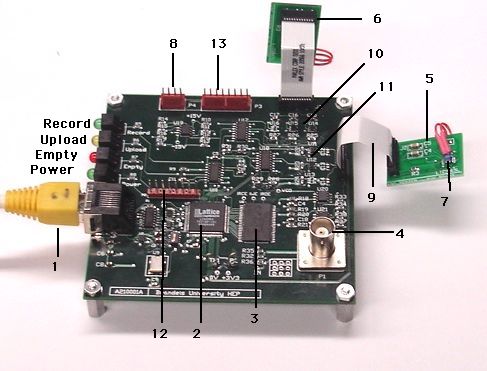
The ADC Tester (A2100) is a LWDAQ device that records the output and power consumption of two ADCs.

Figure: ADC Tester (A2100A) with Two LTC1865L Auxilliary Boards. The flex cables are short for the benefit of the photograph. We give the names of the four indicator LEDs. (1) RJ-45 connection to LWDAQ, (2) programmable logic chip, (3) 512K×8 static RAM, (4) Analog signal input, (5) ADC1 auxilliary board, (6) ADC2 auxilliary board, (7) Pt 1000 RTD glued to LTC1865L, (8) connection for two additional RTDs, (9) 12-way flex cable, (10) fixed voltage supplies for ADC2, (11) fixed voltage supplies for ADC1, (12) logic programming connector, (13) connection to Resistive Sensor Head (A2053L).
Auxilliary Boards
The two ADCs reside on auxilliary boards

Figure: LTC1865L Auxilliary Board. (1) LTC1865L sixteen-bit 250-kHz ADC in MSOP-10 package, (2) 1000-Ω RTD fastened to top side of ADC with super-glue.

Figure: A2100 ADC7982 Auxilliary Board Schematic.
Purpose
- One BNC plug for 50-Ω input from function generator.
- Same fully-differential input to both auxilliary boards.
- ADC common-mode input noise <8 nV/√Hz.
- ADC differential input noise <8 nV/√Hz.
- Four bi-directional logic lines to each auxilliary board.
- Simultaneous, periodic sampling and recording of ADC samples.
- Three stable, fixed 30-mA supplies to each auxilliary board.
- Measurement of current drawn from each fixed voltage.
- Resistive sensor connection to each auxilliaray head.
- Fixed voltages may be turned off as a group.
Entire Apparatus

Figure: ADC Tester (A2100A) with Auxilliary Boards and Low-Temperature Head (A2053L). When we took the picture, we had just cooled ADC2 by immersion in liquid nitrogen, and now the ADC is warming up as it sits above the surface of the liquid. (1) Liquid nitrogen, (2) ADC2 above the liquid, (3) flex cable, (4) ADC1 at room temperature, (5) input from function generator, (6) LWDAQ connection for A2100, (7) RTD cable, (8) LWDAQ connection for A2053L, (9) the Low-Temperature Head (A2053L).
The Sampler Tool is an extension of our LWDAQ Software.

Figure: Sampler Tool. The two traces show the values obtained from two ADCs. In this case, the ADCs are AD7982s. The display range is 1 mV.
Current Measurement
The current measurement channel selects one of eight current measurement channels for analog return, as shown in the following table.
Current
Number
(Hex) | Channel
Name | Command
Word
(Hex) |
|---|
| 0 | VB | 30A0 |
| 1 | VT | 31A0 |
| 2 | VR1 | 32A0 |
| 3 | VA1 | 33A0 |
| 4 | VL1 | 34A0 |
| 5 | VR2 | 35A0 |
| 6 | VA2 | 36A0 |
| 7 | VL2 | 37A0 |
| 8-F | reserved | reserved |
Table: Current Measurement Channels Numbers and Names.
Sample Rate
The sample rate code determines the sample rate for the next sample session.
Sample
RateCode (Hex) | Sampling
Rate (kHz) | Instruction
(Hex) |
|---|
| 0 | 0 | 40 |
| 1 | 1 | 41 |
| 2 | 2 | 42 |
| 3 | 5 | 43 |
| 4 | 10 | 44 |
| 5 | 20 | 45 |
| 6 | 50 | 46 |
| 7 | 100 | 47 |
| 8 | 200 | 48 |
| 9 | 500 | 49 |
| A-F | reserved | reserved |
Table: Sample Rate Codes and Sample Rates
Number of Samples
The number of samples code determines the number of samples in the next session.
Number
of Samples
Code (Hex) | Number of
Samples | Instruction
(Hex) |
|---|
| 0 | ∞ | 50 |
| 1 | 50 | 51 |
| 2 | 500 | 52 |
| 3 | 5000 | 53 |
| 4 | 50000 | 54 |
| 5-F | reserved | reserved |
Table: Number of Samples Code and Number of Samples.
Test ADCs
We tested three ADCs with 4-wire serial interfaces.
| Characteristic |
LTC1865L |
AD7982 |
AD7980 |
| Manufacturer | Linear Technology | Analog Devices | Analog Devices |
| Resolution | 16 Bits | 18 Bits | 16 Bits |
| Package | MSOP-10 | MSOP-10 | MSOP-10 |
| Serial Clock Speed | ≤ 8 MHz | ≤ 80 MHz | ≤ 80 MHz |
| Input |
2 Single-Ended or
1 Differential |
1 Differential |
1 Pseudo-
Differential |
| Data Format | unsigned | signed | unsigned |
| Max Sample Rate |
150 kHz |
1000 kHz |
1000 kHz |
| Operating Temperature |
−40 to 85°C |
−40 to 85°C |
−40 to 85°C |
| Storage Temperature |
−65 to 150°C |
−65 to 150°C |
−65 to 150°C |
| Analog Supply (VCC) |
2.7 V to 3.3 V |
2.5 V |
2.5 V |
| Logic IO Supply |
VCC |
1.8 V to 5 V |
1.8 V to 5 V |
| Reference Voltage |
1 V to VCC |
2.4 V to 5.1 V |
2.4 to 5.1 V |
Table: Manufacturer Specifications.
Test Conditions
We configured our circuits to drive each ADC in the following way.
| Condition |
LTC1865L |
AD7982 |
AD7980 |
| Input |
Single-Ended |
Differential |
Pseudo-Differential |
| Sample Rate |
1 kHz to 150 kHz |
1 kHz to 500 kHz |
1 kHz to 500 kHz |
| Operating Temperature |
−196 to 20°C |
−196 to 20°C |
−196 to 20°C |
| Analog Supply |
3.3 V |
2.5 V |
2.5 V |
| Logic IO Supply |
3.3 V |
3.3 V |
3.3 V |
| Reference Voltage |
3.3 V |
5 V |
5 V |
| Input Range | 0V-3.3V | ±5V | 0V-5V |
| Flex Cable |
15-cm |
15-cm |
15-cm |
Table: Test Conditions.
The AD7982 and AD7980 are pin- and voltage-compatible.
LTC1865 has its own voltages and pin-out.
Experimental Procedure
Thermometer calibration:
−78°C (subliming CO2)
−196°C (boiling N2)
Temperature cycle:
Always start with gentle cool-down
Lower towards liquid nitrogen (cool-down)
Immerse in liquid nitrogen (cold start)
Remove from liquid nitrogen (warm-up)
Observed no damage to any ADC by immersion in N2 liquid.
Replace ADCs and repeat, starting cycle with gentle cool-down.
Voltage Calibration
Checked our voltage calibration by applying known inputs to each ADC.
Stored our data in an Excel spreadsheet.

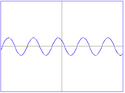
Figure: Response of AD7982 to Sinusoidal Input. The input is ±1 V, 5-kHz, differential. The display range is ±5V, the number of samples displayed is 100. Sampling rate is 100 kHz.
Current Consumption

Figure: Current Consumption of LTC1865L, AD7982, and AD7980 with Sample Rate.
LTC1865L 200kHz

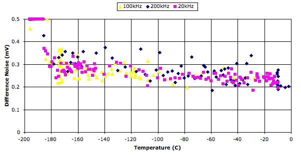
Figure: Difference Noise of LTC1865L with Temperature for Various Sample Rates. The ADCs are reading IN− as a single-ended input, and there is no signal applied to IN. We clip the difference noise to a maximum value of 0.5 mV so we can see the failure points at the top of the graph.
AD7982 200kHz

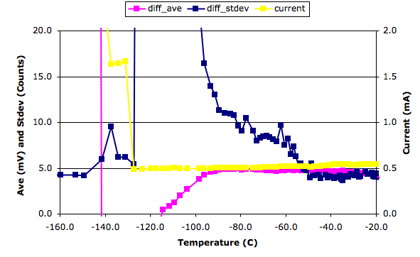
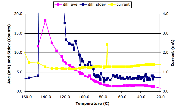
Figure: Affect of Temperature upon AD7982 with No Input. Sampling rate is 200 kHz. We plot total current consumption of the chip, the standard deviation of the difference between the cooled and room-temperature ADCs in 18-bit counts, and the average difference in mV. Both ADCs convert IN as a differential input. Raw data here.
AD7980 200kHz

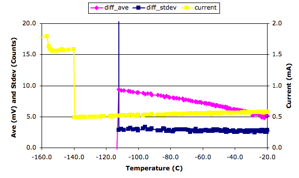
Figure: Affect of Temperature upon AD7980 with No Input. Sampling rate is 200 kHz. We plot total current consumption of the chip, the standard deviation of the difference between the cooled and room-temperature ADCs in 16-bit counts, and the average difference in mV. Raw data here.
AD7982 500kHz

Figure: Affect of Temperature upon AD7982 with No Input. Sampling rate is 500 kHz. Raw data here.
Conclusion
The ACDs sustained no damage when operated at −196°C.
The LTC1865L operates well down to −180°C: 200 kHz @ 350 μA, noise <2 16-bit counts with single-ended input. Fails at −190°C. Can re-program ADC Tester to run LTC1865L in differential mode for less noise.
The AD7982 operates well down to −60°C: 200 kHz @ 500 μA, 500 kHz @ 1.4 mA, noise <5 18-bit counts. Noise increases until failure at −100°C.
The AD7980 operates down to −100°C: 200 kHz @ 500 μA, noise <5 16-bit counts, DC offset shifts by 5 mV from 0°C. Fails suddenly at −110°C.
The LTC1865 operates from 5V, runs at >250 kHz. Could use two of these to make 500 kHz and run at −140°C with confidence.
