TCPIP-VME Interface (A2087) Manual
©2019-2021, Kevan Hashemi, Brandeis University
©2024, Kevan Hashemi, Open Source Instruments Inc.
Contents
Description
Design
Operation
Current Consumption
Test Pins
Development
Description
[13-MAY-24] The TCPIP-VME Interface (A2087) is a VME Master with a TCPIP interface that allows us to communicate with VME Slaves over a wired TCPIP connection.

Figure: LWDAQ Relay with VME Interface (A2087A). Showing (1) configuration switch, (2) face plate, (3) insertion and removal latches, (4) RJ-45 socket, (5) indicator lamps, (6) reset switch, (7) VME backplane connector P1, (8) backplane connector P2, (9) RCM6700 embedded computer, and (10) serial number label.
We communicate with the A2087 using LWDAQ TCPIP messages. The A2087 handles its TCPIP communication with an RCM6700 embedded microprocessor. The A2087 hardware is capable of providing the following VME functions, depending upon its firmware.
- When loaded in Slot 1, performs single-level (SGL) bus arbitration.
- When loaded in Slot 1, performs interrupt arbitration for IRQ7.
- 16, 24, and 32-bit address cycles (A16, A24, and A32).
- 8, 16, and 32-bit data cycles (D08, D16, and D32).
- Asynchronous read and write driven by DTACK.
- Bus error timing.
- System reset generation.
- As a slave, generates IRQ7 interrupts upon TCPIP command.
- As a slave, provides access to TCPIP message buffer.
Our intention is to implement these functions in the P2087 controller firmware and C2087 relay software as we require them. The hardware version resistors, R22-R24, are intended to configure the board for various VME functions, such as master, slave, and arbitrator. The following versions of the A2087 exist.
| Version | Function | VME Role |
|---|
| A2087A | LWDAQ Relay | A24 bus master for A2037A and A2071A slaves |
Table: Versions of the TCPIP-VME Interface (A2087). We list the VME role performed by each.
The A2087A is designed to replace the TCPIP-VME Interface (A2064). The A2087A communication with VME-resident LWDAQ controllers, such as the A2071A or A2037A. The A2087A is equipped with firmware P2087A and software C2087A. The A2087A acts as a VME master. It implements only 24-bit addressing (A24 in VME terminology) with non-privileged access (address modifier 0x39), and it implements only single-byte reads and writes. It does not handle interrupts in any way. It does not permits bus arbitration, but acts as the sole master for the VME backplane. It implements the LWDAQ base address in a manner backward-compatible with earlier LWDAQ relays, such as the A2064A. As a consequence of its backward-compatible base address implementation, the A2087A is incapable of writing to any VME address with least significant byte in the range 42-45.

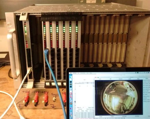
Figure: LWDAQ Relay (A2087A) and LWDAQ Controllers with VME Interface (A2071A) in 6U, VME-64 Crate. Data acquisition is taking place through a local network to a laptop.
The A2087 will operate equally well in a 6U VME-64 crate, 6U VME-32 crate, or a 6U VME-24 crate.
Design
Note: All our schematics and Gerber files are distributed under the GNU General Public License.
S2087_1: RCM6700 Logic.
S2087_2: VME Data.
S2087_3: VME Address.
S2087_4: VME Controller.
S2087_5: Power Supplies.
A208701A: Printed circuit board version A.
A2087A.ods: Bill of Materials for A2078A.
Code: Firmware and software source files and object files.
RCM6700: Embedded microprocessor manual.
VME Bus 32-Bit: ANSI VME Backplane Specification (01-OCT-1985).
VME Bus 64-Bit: ANSI VME Backplane Specification (10-APR-1995).
Operation
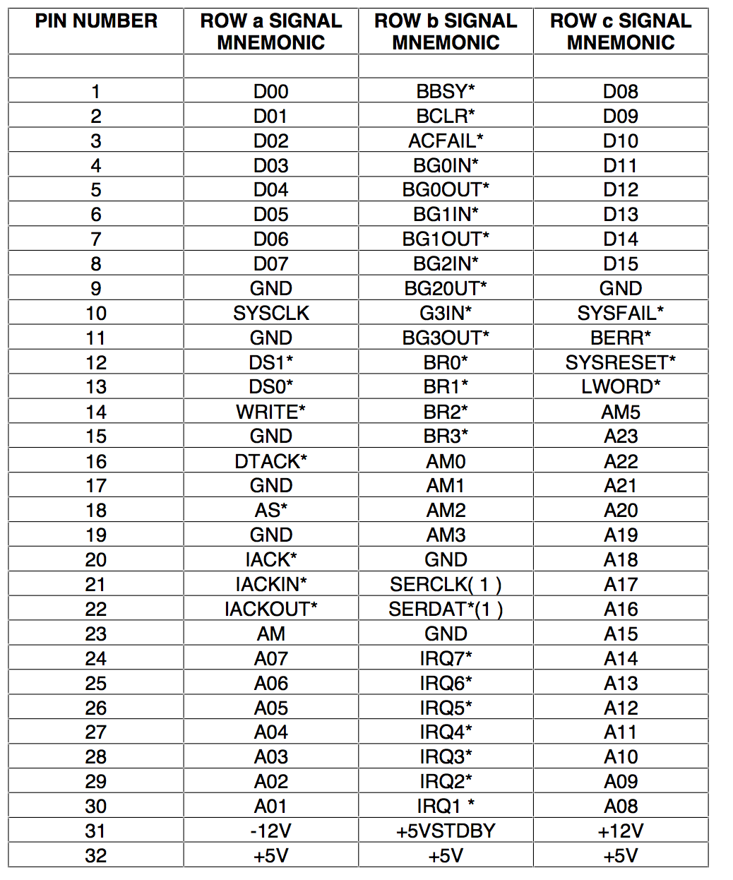
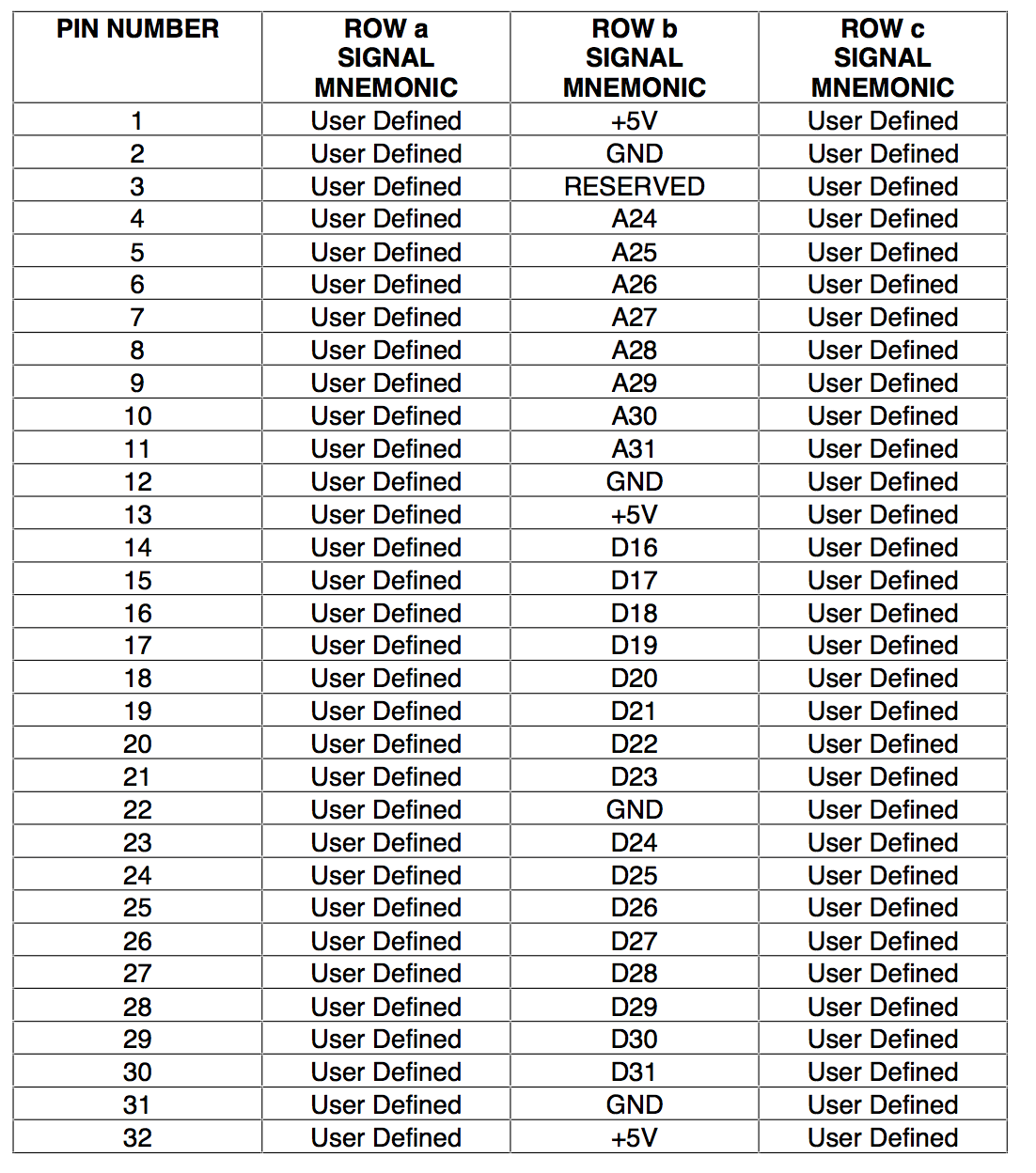
[19-APR-21] The A2087 provides a TCPIP interface with a VME backplane. It mates with VME connectors J1 and J2. Both J1 and J2 are 96-way DIN sockets. On the A2087 are two right-angle 96-Way DIN plugs. The top one is P1, which mates with J1. The bottom one is P2, which mates with J2. The A2087A may be installed in a VME-64 crate, but does not make use of any of the additional VME-64 connections.

Figure: VME P1/J1 Connections.
The TCPIP interface is provided by an RCM6700 embedded computer. The TCPIP interace presents a static IP address, by default 10.0.0.37. We can program with the Configurator Tool to use any IP address we like.

Figure: VME P2/J2 Connections.
We can restore the IP address of the RCM6700 to 10.0.0.37 by pressing the reset and configuration switches at the same time, then releasing the reset switch to allow the RCM6700 to boot up and notice that we are pressing the configuration button, at which point it will re-write its configuration to the default values, which includes setting the IP address to 10.0.0.37.
The A2087A is a TCPIP-VME Interface for use in VME-based LWDAQ systems. It replaces the A2064. The A2087A provides the following LWDAQ Controller address map, which is accessible to the LWDAQ Software through byte_write, byte_read, and stream_read instructions. The LWDAQ Controller addresses appear on the VME Backplane. They are the same as twenty-four the bit VME addresses.
| Address (Hex) |
Address (Decimal) |
Contents |
Read-
Write |
| 00000000 | 0 | Hardware Identification Number (87) | R |
| 00000012 | 18 | Hardware Version Number (0-7) | R |
| 00000013 | 19 | Firmware Version Number (1+) | R |
| xxxxxx2A | 42 | VME Address Register 3 (A24-A31) | W |
| xxxxxx2B | 43 | VME Address Register 2 (A16-A23) | W |
| xxxxxx2C | 44 | VME Address Register 1 (A8-A15) | W |
| xxxxxx2D | 45 | VME Address Register 0 (A1-A7) | W |
| 0000003F | 63 | data portal | R |
Table: LWDAQ Controller Address Map of the A2087A. An "x" in an address means "don't care". The LWDAQ controller address consists of the LWDAQ base address plus a one-byte
The LWDAQ Software's byte_write instruction carries only the lowest eight bits of the LWDAQ controller address. The upper twenty-four bits are stored in the address registers 1-3, having been written by earlier byte_write instructions to addresses 42-44. The A2087A intercepts byte_write instructions to any of the addresses 42-45, and uses these instructions to set its internal VME address registers instead of executing a VME backplane write cycle. This behavior is backward compatible to that of earlier LWDAQ relays, such as the A2064, but not identical. The A2064 would write to VME address locations while setting its own base address registers, so that the upper three bytes of the VME address would change during the write cycle. The A2064 was incompatible with any VME slave that implemented addresses with least significant byte 42-45, because such slaves could be written to at any time while the base address was being altered. The A2087A is incapable of writing to these same addresses, so it is incompatible with any slave that requires such addresses to be written. But the A2087A will not cause any unintended activity on such slaves during writes to its base address registers. If we want to use the A2087 with generic VME slaves, we must implement a new set_base_address operation that will set the three base address registers without any VME activity, and then permit the A2087 to read and write to the 42-45 addresses with the existing byte_write instruction.
The top address byte is driven onto the VME backplane for A24-A31, but the A2087A implements only twenty-four bit addressing on the VME backplane, so only the A8-A15 and A16-A23 base address bytes play a part in selecting a LWDAQ controller card. These cards will be configured with base addresses of the form 00xxxx00. If they have a !LADDR switch (long addressing), it must unasserted to select A24 addressing instead of A32. When the top three bytes of the base address are zero, the A2087A provides a hardware ID, hardware version, and firmware version in response do byte_read instructions to addresses 0, 18, and 19 respectively. A stream_read from the data portal will produce an incrementing value 0-255, which will generate a gray-scale image in the Camera Instrument if we set daq_image_width to 256.
Internal to the A2087A is the VME Controller Address Map by which the RCM6700 implements VME access cycles. The VME Controller Address Map appears in the external input-output address space of the RCM6700, and so may be accessed directly by the microprocessor.
| Address (Hex) |
Address (Decimal) |
Contents |
Read-
Write |
| 28 | 40 | Configuration Switch (0 or 1) | R |
| 2A | 42 | VME Address Byte 3 (A24-A31) | W |
| 2B | 43 | VME Address Byte 2 (A16-A23) | W |
| 2C | 44 | VME Address Byte 1 (A8-A15) | W |
| 2D | 45 | VME Address Byte 0 (A1-A7) | W |
| 2E | 46 | VME Address Control Register: AM5-AM0, !WRITE, !LWORD | W |
| 2F | 47 | VME Control Register, DS0, DS1, AS | W |
| 2F | 47 | VME Status Register, DTACK, BERR | R |
| 30 | 48 | VME Data Byte 3 (D24-D31) | RW |
| 31 | 49 | VME Data Byte 2 (D16-D23) | RW |
| 32 | 50 | VME Data Byte 1 (D8-D15) | RW |
| 33 | 51 | VME Data Byte 0 (D0-D7) | RW |
Table: VME Controller Address Map of the A2087A. These addresses are mapped into the RCM6700's external input-output address space.
When the RCM6700 in the A2087A executes a byte_write to write to a VME location, it does not set the A8-A31 address registers, but assumes these have already been written by byte_write instructions to the address bytes. Instead, the RCM6700 writes the eight-bit address provided by byte_write to VME Address Byte 0. If the address is even (A0 = 0), the RCM6700 writes the byte_write data to VME Data Byte 1, otherwise it writes to VME Data Byte 0. The RCM6700 writes 0xA7 to AM0-AM5, !WRITE, and !LWORD in the VME Address Control Register at location 46, specifying an A24, non-privileged write cycle for two or fewer bytes of data. The relay writes the correct values of DS0, DS1, and AS to the VME Control Register at location 47. On a single-byte access at an even location, the relay asserts DS1 and AS by writing 0x06. On a single-byte access at an odd location, the relay asserts DS0 and AS by writing 0x05. The slave will now respond, and when the slave is done, it will assert DTACK. The relay reads location 47. When the value it receives is non-zero, either BERR or DTACK has been asserted. The write access either succeeded or failed, but it is in any case complete.
The execution of a LWDAQ byte_read instruction is similar. Instead of writing 0xA7 to the VME Control Register, the RCM6700 writes 0xE7 to unassert !WRITE. Instead of writing a data byte to one of the data registers before the start of the cycle, the RCM6700 reads the data byte out of a register at the end of the cycle.
The same VME Controller registers can be used to implement two-byte and four-byte VME access cycles, although these access cycles are not implemented in the A2087A. In a single-byte write to an even address (A0 = 0), the relay writes to data byte 1 at location 50. In a single-byte write to an odd address (A0 = 1), the relay writes to data byte 0 at location 51. In a two-byte write to an even address (A0 = 0), the relay would write the most significant byte to byte 1 at location 50 and the least significant byte to byte 0 at location 51. In a four-byte write to an even address (A0 = 0), the relay would assert LWORD by writing a 0 to !LWORD in the Address Control Register. Now it would write the four data bytes to VME Controller locations 48-51 in little-endian order: most significant byte first. On a two-byte access at an even location, the relay would assert DS0, DS1, and AS by writing 0x07 to the VME Control Register. In order to implement these access cycles, we would add them to the relay software (C2087A02.c) and add commands to the LWDAQ software (Driver.tcl).
Current Consumption
[19-NOV-19] The A2087A draws 950 mA from the VME backplane's +5 power supply. Of this, 720 mA is the logic and VME interface buffers, 230 mA is the RCM6700 embedded processor. The A2087A does not use the ±12 V power supplies.
Test Pins
Test pins TP1 to TP8 are available on a SIP-12 connector behind the test lamps. The test pins are connected to the four amber and four red LEDs. When the lamp turns on, the test pin signal is Hi. The test pin definitions are given below, by this ABEL code excerpt. We have OR as #, NOT as !, XOR as $.
TP1  = CSW $ LNK;
TP2  = BAZ;
TP3  = DEN0 # DEN1 # DEN2 # DEN3;
TP4  = !DCK0 # !DCK1 # !DCK2 # !DCK3;
TP5  = DDIR;
TP6  = !ACK0 # !ACK1 # !ACK2 # !ACK3 # !ACK4;
TP7  = DTACK # BERR;
TP8  = CDS;
With these definitions, the front panel lights show clearly when data is passing into the VME backplane, and when it is coming out. The combined Configuration Switch and Link indicator flashes when we have ethernet activity and when we press the configuration switch.
Development
[01-APR-19] Schematic complete.
[22-JUL-19] Printed circuit board A208701A arrived.
[26-SEP-19] Firmware version three (FV3), defined by P2087A03, combined with software version two (SV2), defined by C2087A02, provides the first fully-functional TCPIP-VME Interface for use with VME-resident LWDAQ systems. We can replace one of our A2064A interfaces with the A2087A and read out a camera attached to the VME crate with no change in the LWDAQ data acquisition settings. We check the stream write and stream delete functions of the RCM6700 software using a Toolmaker script and our Driver Checker program.
[16-OCT-19] Firmware version four (FV4) provides better test pins. We have two new and fully-functional A2087A circuits tested.
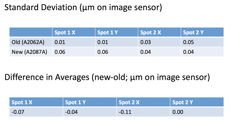
[07-NOV-19] We set up an N-BCAM and take images of its two lasers using an A2071A VME-resident controller and an A2064A VME-resident relay. We switch to A2087A VME-resident relay and take images again. We compare the images taken through the two interfaces.

Figure: Agreement Between Images Downloaded Through New (A2087A) and Old (A2064A) Relays.
[11-NOV-19] Firmware P2087A04 did not manage the VME backplane's !SYSRESET signal, which we abbreviate to !SYSRST in the schematic. The GQ4 output was floating HI, turning on Q4, and asserting SYSRST. The A2087A was working with our prototype A2071A, but only because the SYSRST signal is disconnected on that particular assembly. With all other A2071A, the A2087A was resetting the VME interface on the A2071A all the time. Firmware P2087A02 fixes the problem. We produce firmware P2071A02, which takes !SYSRST and drives the local !RESET line, so that we can reset all A2071As in a crate with the button on the A2087A.
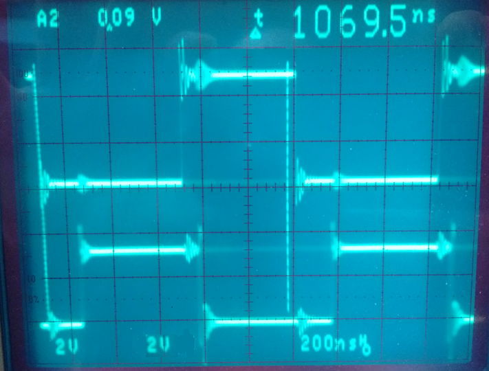
[14-NOV-19] We perform block delete and block read operations through the A2087A with firmware P2087A04 and software C2087A02, reading from A2071A, which asserts DTACK 164 ns after DS on both read and write cycles. Each read cycle takes 1105 ns, each write cycle takes 1064 ns.

Figure: !DS on VME Backplane (top) and DTACK on Test Point 7 (bottom), For VME Read.
The C2087A02 software implements the read loop with the following assembler code.
ld b,0x00
ld hl,(io_addr)
ioi ld (iy),0x00
outer_loop_sr:
    inner_loop_sr:              ;0
        ld a,(vcr_value)        ;7
        ioe ld (ix),a           ;11 + w
        ioi ld (iy),0xFF        ;12
        dtack_ilsr:             ;0
            ioe ld a,(ix)       ;9 + w
            cp 0                ;4
        jr z,dtack_ilsr         ;6
        ioe ld a,(hl)           ;7 + w
        ld (de),a               ;7
        ioi ld (iy),0x00        ;12
        ioe ld (ix),0x00        ;12 + w
        inc de                  ;2
        dec b                   ;2
    jr nz,inner_loop_sr         ;6 Total 99 + 4w = 127
    dec c
jr nz,outer_loop_sr
The total VME read cycle takes 127 cycles of the RCM6700 187 MHz clock. We expect the total read cycle to take no more than 680 ns plus the DTACK delay of 160 ns is 840 ns.
[20-NOV-19] We plug an A2087A equipped with firmware FV=5 and software SV=2 into a VME-64 crate and operate both A2071A and A2037A VME-resident controllers successfully.
[05-DEC-19] Our VME-64 crate consumes 1.5 A from +5 V and 0.0 A from ±12 V with no VME cards inserted. We believe this current is passing through the termination resistors on the 64-bit data bus and the 64-bit address bus. We plug in the A2087A and add 0.4 A from +5 V and 0.0 A from ±12 V. We plug in one A2071A controller and add 0.4 A from +5 V and 0.13 A from ±12 V. An A2037A controller adds 0.5 A from 5 V and 0.10 A from ±12 V.
[06-JAN-20] For three weeks we have been running a once-a-minute exercise of our A2087A in VME-64 crate with 8 LWDAQ Controllers (A2071A) and one LWDAQ Controller (A2037A). The process is still running. We see the head power lights switching on all nine controllers once a minute.
[19-FEB-20] A crooked U17 had a short from 3V3 to 0V on its case. The 3V3 buck converter was waiting for the short to end. The SN74ABT646s were all powered up with +5V. But all their enable inputs were asserted by U1, which had no power. Devices U3, U4, and U9 became excessively hot. We replace these, and board works. We have already sent X00043 to CERN. Today we are sending X00044 and X00045 as well as a programming cable for the firmware on A2071A controllers.
[12-MAY-21] We now have eight A2087A at CERN. One has been in use for a year. The others are awaiting installation in the ATLAS nSW readout and in test stands.

