 Fiber Positioner Circuits (A2089)
© 2019-2020, Kevan Hashemi, Brandeis University HEP© 2021, Kevan Hashemi, Open Source Instruments Inc
© 2019-2020, Guadalupe Duran, Brandeis University HEP
Notice: Starting January 2022, our fiber positioner work continues at Open Source Instruments Inc., funded by National Science Foundatin (NSF) SBIR grant number 2111936. For latest work see here.
[10-NOV-20] We use assembly number A2089 for a family of medium-voltage power supplies and amplifiers that drive piezo-electric (PZ) actuators, as well as mounting platforms for the same actuators. In particular, we are focused on tube actuators that bend when we apply voltages to four longitudinal quadrant electrodes. Our plan is to mount a rigid support pipe in the end of the PZ tube, run an optical fiber through the tube and the pipe, and so use the PZ tube to move the fiber tip around. With such fiber positioners arranged in the focal plane of a telescope, we can hope to align a large number of fibers with separate galaxy images, and so obtain their spectra simultaneously.

In Properties of Piezoelectric Tube Actuators for use in a Fiber Positioner for a Spectroscopic Telescope, we use the A2089 circuits to study the stability, precision, and accuracy of direct fiber positioners. We conclude that an absolute accuracy of 10 μm over a 3-mm diameter operating range is a realistic expectation from such a system, provided it is well-calibrated, and provided the formidable challenge of controlling each actuator continuously and independently can be met. In Fiber Positioning System Results: General Behavior, Creep Mitigation, and a Set Start Point we show how we can mitigate the effect of creep by adjusting the actuator voltage. In Fiber Positioner System: A Method to Guide 30,000 Optical Fibers, we describe how a spiral reset procedure allows us to overcome hysteresis in the piezoelectric actuator.

The PT230.94 has a 500-μm wall thickness. Four quadrant electrodes are distributed around the outer radius, and one electrode on the inner radius. The permitted drive voltage for each outer electrode with respect to the inner electrode is ±250 V. The above figure shows the deflection that results from +250 V applied to one side and −250 V applied to the other. Another PZ tube we had custom-made by PI Ceramic, is 40 mm long with 3.6 mm outer diameter and 2.8 mm inner diameter. It is designed to accept a 2.6 mm diameter hypodermic steel tube with a 2.5 mm diameter zirconia ferrule glued at the tip to present the optical fiber tip. The maximum bend in the 40-mm tube is roughly 3.1 mrad.
| Parameter | Value | Comment |
|---|---|---|
| Fiber Spacing | 5 mm | spacing between fibers in a square grid array |
| Fill Factor | π/4 = 79% | fraction of array area accessible to at least one fiber tip |
| Positioning Accuracy | 20 μm | absolute accuracy of fiber center placement |
| Positioning Time | 100 s | time to re-locate all fibers with specified accuracy |
| Fiber Holder Diameter | 1 mm | the diameter of the tube holding the fiber |
| Power Dissipation | 10 mW/fiber | the dissipation in the local drive electronics |
Our objective is to build a fiber-optic positioning system meeting the above specification. On a 500-mm square focal plane, we would be able to place ten thousand fibers. A 1-m focal plane will provide fifty thousand fibers. All piezo-tubes are driven continuously by a constant voltage that dictates and maintains its fiber position. Piezo crystals themselves present a resistance of hundreds of GΩ, so their inherent current consumption when they are doing no work is tens of nanoamps. The circuit below is an example of a slow, low-power driver for a piezo-tube electrode.

To drive the four quadrants of a single piezo-tube, we use a digital to analog converter (DAC) such as the DAC104S085, which provides four twelve-bit outputs at a cost of 1.1 mW current consumption from 3.3 V. In the above circuit, we have the 0-3.3 V DAC output C on the base of Q1. The current I1 will be roughly (C−0.6)R1, or 0.0-1.0 μA. This current passes through R2 and D1, setting the base voltage of Q2 with respect to +250 V, and giving rise to I2 of 0.0-5.0 μA. This current passes through a 100-M&Ohm; resistor to −250 V, so that the voltage at P varies from −250 V to +250 V as we vary C from 0.6 V to 3.3 V. The maximum power dissipation of the circuit is 5 μA × 500 V = 2.5 mW. We plan for opposite electrodes to be driven with opposite voltages, so the power dissipation for the East-West electrodes will be 2.5 mW for all positions, and for North-South another 2.5 mW. Add to this the 1.1 mW of the DAC and another 0.2 mW for a micropower logic chip such as the LCMXO2-1200ZE, the maximum power dissipation per piezo-tube should be around 6 mW, so we make 10 mW/fiber our target, to give us some room for error.
The capacitance between a PT230.94 piezo-tube electrode and the grounded inner electrode is around 3 nF. With a 5-μA charging current, the voltage across this capacitance will vary at 1700 V/s. If the piezo-tube has to move a 1-g mass a distance of 1 mm vertically, it will need a total of 10 μJ of energy, which a 1-μA current will supply in one second even if the voltage across the piezo crystal is only 10 V. The above circuit is both powerful enough and fast enough to support movement of the fibers to a new position in less than a few seconds.
[17-JUL-19] The A2089A is a static piezo-electric driver consisting of a ±250 V power supply and two hand-operated multi-turn potentiometers to set each of the two output drive voltages to a value −250-+250V.
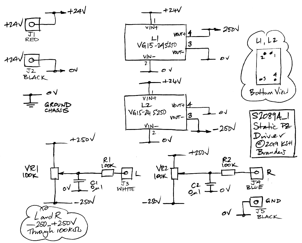
The circuit is powered by 24 V delivered through two banana jacks. Two VG1524S250 isolated DC-DC converters produce +250V and −250V from the 24-V input.
The ±250-V voltages are higher than we are used to working with in an open-frame circuit. We touched the +250-V and −250-V power supplies with one finger, while holding a ground terminal with the other hand, and felt only a slight sensation. To make sure that the outputs are safe for use without special precautions, they are presented to banana sockets through 100-kΩ resistors. The resistors limit the current through the human body to less than 2.5 mA. A typical hand-to-hand resistance in the body is 100 kΩ. Such a body resistance would pass no more than 1.2 mA from the R or L outputs, dissipating roughly 100 mW of power.
The A2089A allows us to connect ±250 V to two opposite electrodes on a PZ tube and so cause static displacement of a fiber pipe glued into the tube.
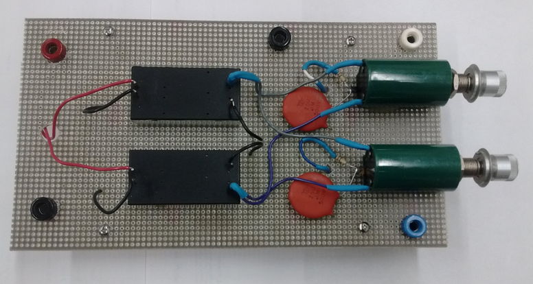
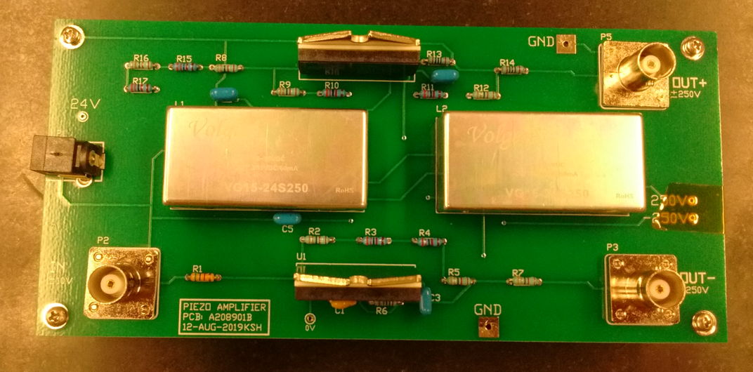
[18-JUL-19] The A2089B provides two inverting amplifiers with output dynamic range ±250 V. Each amplifier has gain −25. We connect two function generator signals to LIN and RIN and so obtain two amplified signals a LOUT and ROUT respectively. Signals are brought to and from the board with vertical BNC sockets. Power for the amplifier comes from a 24-V power adaptor with 5.5-mm center-positive plug.
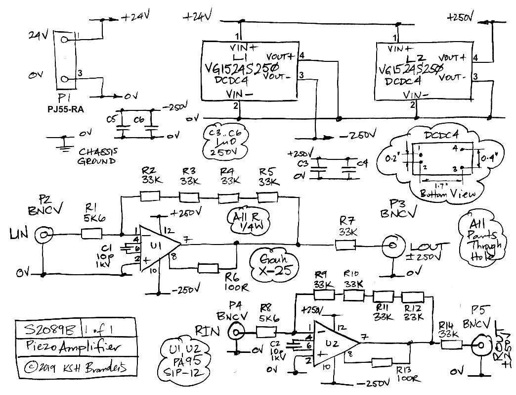
The ±250-V power supply is produced by two VG1524S250. Amplification is provided by the PA95U high-voltage power operational amplifier. The exposed metal backs of the two amplifiers U1 and U2 are connected to their output ports, so avoid touching these when the output signal is large. The A2089B draws roughly 200 mA from its 24-V power supply.

The A208901A printed circuit board has two errors. One is an inversion of the footprint for L1 and L2, which we get around by mounting the two converters on the bottom side of the board. The other is a reversal of the connections to P1. We correct this reversal by cutting tracks and adding wire links.
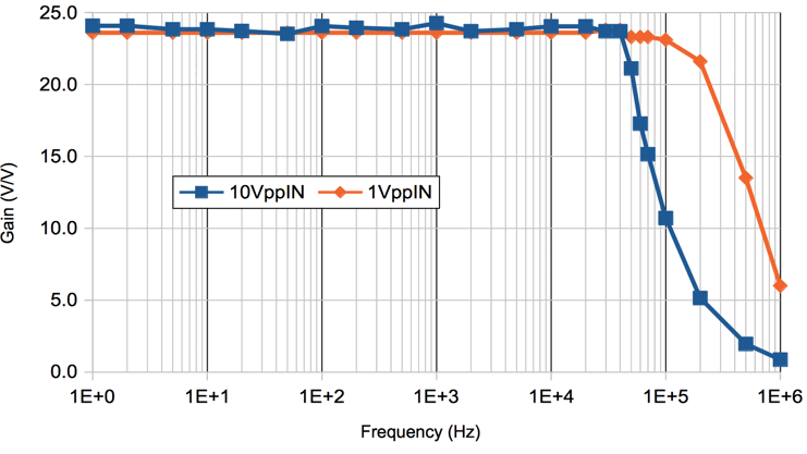
We apply a 1-Vpp sinusoid and a 10-Vpp sinusoid to RIN and observe the amplitude of ROUT. For the 10-Vpp input, we see slew-rate limiting of the output starting at around 20 kHz. The PA95U has a typical slew rate of 30 V/μs with a 4.7-pF compensation capacitor. We are using 10 pF and we see a 20 V/μs maximum slew rate.
[14-AUG-19] The A2089B2 is a modification of the A2089B where R1 = 130 kΩ so that the gain of the U1 amplifier from P2 to P3 is −1. We connect a signal to RIN. We connect ROUT to LIN. Now we see RIN multilied by +25 at LOUT and −25 at ROUT. Thus the A2089B2 provides complimentary drive output for two PZ electrodes using one signal.
We use a BNC-T on the ROUT socket so as to share it between the PZ electrode and LIN. We connect ×10 oscilloscope probes to the output resistors of both the left and right channels so as to view the output signals.
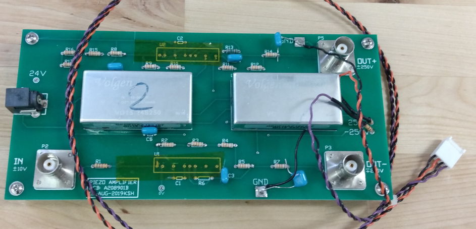
[12-AUG-19] The A2089C provides two complimentary ±250-V outputs generated from one ±10.6-V input. The OUT+ signal is +23.6 times the input, the OUT− signal is −23.6 times the input. The time constant of the driver's step response iss 130 ms, making it more than fast enough to support our fiber-positioning work, but slow enough to avoid exciting the natural frequency of the fiber support structure. The driver allows us to generate the complimentary East-West or North-South drive voltages for a PZ tube, such as the PT230.94, from a single input signal.

The A2089C printed circuit board (the A208901B) provides an extension with six footprints designed for solder-mounting of six PT230.94. Each footprint is supplied with the same east, west, north, and south drive voltages from four BNC sockets.
The A2089C amplifiers are identical to those of the A2089B, except one is connected with gain −1 to the output of the first amplifier, thus producing the gain of +25 to compliment the first amplifier's gain of −25.
[12-SEP-19] We load connectors and standoffs onto a PZ Support Plate and solder a PZ actuator with steel tube into one of the PZ footprints. We injure a thumb pressing upon the ±250 V test points on the amplifier board. When the two points are close enough, the current through the skin is significant and causes nerve damage. We cover the test points with kapton tape.
When we apply complimentary 1-Hz 250-V amplitude sine waves to the East-West electrodes, we see the tip of our 300-mm long, 1.25-mm diameter steel tube, which is soldered into the tip of the PZ tube, moving with a peak-to-peak amplitude of around 1.4 mm.

As we increase the frequency from 1 Hz, the amplitude of the movement increases until we appear to arrive at a resonance at around 12 Hz, where the peak-to-peak movement of the fiber tip starts to exceed 30 mm and we turn off the excitation voltage. Above 12 Hz, the amplitude reduces.
[13-SEP-19] We consider how important is the range of motion of the optical fiber tip as compared to the spacing of the fibers in an array. Our prototype array has a two-dimensional 5-mm spacing, and the range of motion of the fiber is 1.4 mm. Suppose we focus a region of the sky onto a rectangular plane of width b and height a. We place in this rectangle our array of optical fibers. Each fiber can move in a circle of diameter d, and the centers of these circles are arranged in a two-dimensional array of spacing w. Thus there are a total of ab/w2 fibers in the image rectangle.
Within the image rectangle we suppose there are n celestial objects arranged at random. We ignore the fact that some may be too close together to distinguish with a fiber of finite diameter. Any object within the range of motion of a fiber may be viewed by that fiber.
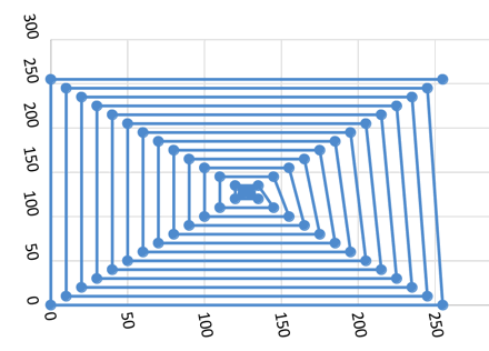
We prepare a simulation program, Observing.tcl, a TclTk script we can run in the LWDAQ Toolmaker. The simulation begins by plotting the n objects as black dots to indicate that they have not yet been observed. We place the center of top-left fiber's range at the top-left corner of the image rectangle. We go through all the fiber circles and pick one unobserved object to observe, and mark it as red to show it has been observed. If not unobserved object exists in the fiber range, the fiber makes no observation.
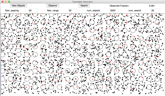
We repeat this procedure, but now we displace the center of the top-left fiber range by one half the diameter of the range to the right. In subsequent exposures, we continue to displace to the left, and then downwards, so as to move the fiber range in a regular pattern that covers all locations. After each observation, we record the fraction of the n objects that have been observed. We plot this fraction versus the number of exposures. We do this for various values of d/w.
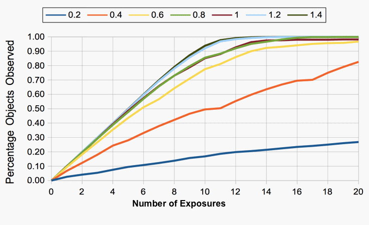
To observe 90% of the available objects, it takes 10 exposures with d/w = 1.2 or 1.4, and 11 exposures with d/w = 0.8 or 1.0. With d/w = 0.6 it takes 13 exposures. For lower ratios, the number of exposures required increases rapidly. The fact that the performance for a ratio of 0.8 equals that of 1.0 we suspect is an artifact of the way we are displacing the fiber array.
We try another algorithm for displacing the fiber array between exposures. Before each observation, we place the fiber array at random, with the top-left fiber somewhere in a square of side w at the top-left corner of the image rectangle. We obtain our plots of observed fraction versus number of exposures for various ratios of fiber range to fiber spacing. We find that random translation gives better performance for ratio 1.0, which suggests our regular translation is flawed.
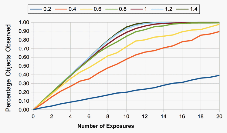
When we have an average of 10 objects in each square the size of one fiber spacing, the number of exposures required to observe 90% of objects is 10 for fiber range 1.2 times the spacing, and 13 for fiber range only 0.6 times the spacing. There is no advantage gained when we increase the range to 1.4 times the spacing.
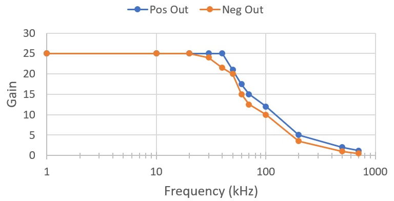
[17-SEP-19] We measure the gain versus frequency of our first A2089C, shown below.
[23-SEP-19] We have two PT230.94 tubes joined together with wires soldered to their electrodes, making a 60-mm tube. We have a 1.25-mm diameter, 300-mm long steel tube glued into the top end of the top tube. The bottom of the bottom tube is soldered to one of our support plates. We apply ±250 V complimentary 1-Hz sinusoids to the East-West electrodes and take the following movie of the tip of the fiber.
By comparing the movement of the tube to its diameter as seen in the video, we deduce that the center of the tube is moving a total of 5.0 mm, or 100% of the fiber spacing.
[08-OCT-19] We consider the deflection of the end of our fiber guide tube when it is horizontal, as shown in the derivation below.

Using the above result, we obtain the following deflections for two varieties of stainless steel tube available from MicroGroup, and a hypothetical carbon fiber tube.

It is not possible to make carbon fiber tubes with walls as thin as a the steel tubes listed in the table above. In the derivation below, we show that the deflection of a thin-walled tube is independent of the wall thickness.
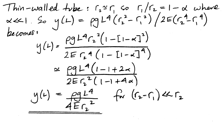
Even with thin walls, however, the stainless steel tube bends four times farther under its own weight than the carbon fiber tube.
[24-MAR-20] We add capacitors C9 and C10 to our two A2089C Piezo Drivers. Without these capacitors, the op-amps sometimes latch up at +250 V when we switch IN from positive to negative with a step. The capacitors give the amplifiers a time constant of 130 ms. We connect two A2057H input-output heads to provide IN from their Y1 outputs, and to monitor North, South, East, and West of a single PZ tube.
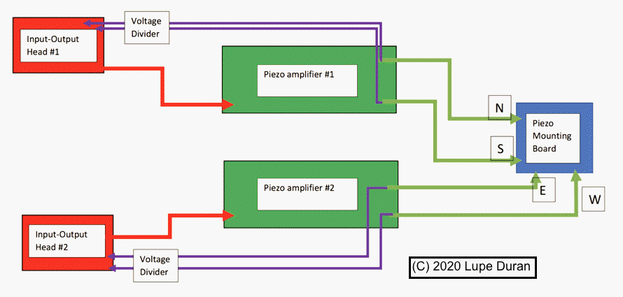
[15-SEP-20] We perform experiments with a single PZ tube using our remote control test stand. We have two Input-Output Heads (A2057H) and two Piezo Drivers (A2089C) providing drive voltages and monitoring. Each A2057H has been configured to generate a voltage ±10 V, and is equipped with a ÷28 voltage divider on each of its two analog inputs, so that their ±7.5 V range can cover ±210 V drive voltage. We would rather have used a ÷40 divider, but we believed analog input range was ±10 V when we designed the divider.
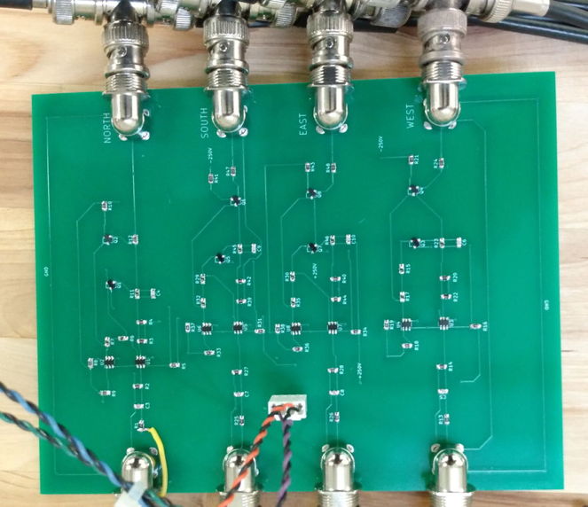
[04-MAR-20] We have ten 40-mm long PZ tubes, inner diameter 2.8 mm, outer diameter 3.6 mm. We submit the following circuit board for fabrication, in which we provide mounting footprints for nine such tubes, named C1-C9. The circuit boards should be delivered to Brandeis by Friday 13th March.
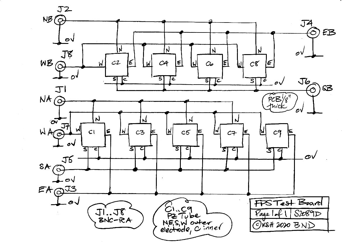
The nine tubes are divided into two sets A and B consisting of 5 and 4 tubes respectively. All of set A have the same NA, EA, SA, and WA voltages on the top, right, bottom, and left electrodes respectively. All of set B are driven by NB, EB, SB, and WB.

The board finish is ENIG, which has an outer gold plate, and allows us to be confident in the diameter of the plated through holes. The PZ footprints have holes 2.79 mm in diameter, or 0.110". The board itself is 0.125" thick. We plan to put the board up on 1/4" standoffs, then insert a 7/64" = 0.109" diameter, 0.5" long steel pin into the hole, so it sticks up 0.125" above the top surface of the board. We then slide the PZ tube over the pin to position it for alignment and soldering. We pull the pin out of the bottom side after we are done, and we can then solder the inner surface electrode to the plated through hole if we want to, and so ground it.
We apply the above spiral reset procedure to our actuator tube before we move to a new position. We move to a given end position from a random start position by inserting this procedure between the start position and end position. We have two actuators equipped with fibers, and we try various end positions. Our precision moving to the given position is better than 20 μm rms at the fiber tip, and is dominated by drift during the course of each experiment. We plan to determine if the drift is caused by temperature changes, amplifier drift, or is a property of the actuator tube itself.
[15-JUL-20] Our Slow, High-Voltage Amplifier (A2089E) is designed to drive piezo-electric actuators with a time constant of order one second with electrode voltages −250 to +250 V.

We bring ±250 V power onto the board with a four-way shrouded header, Molex part number 0705430003, which is rated for operation at 250 V. We have +250V on P1-2, and −250V on P1-4, with 0V on the remaining pins. The connector is polarized, so we hope to avoid connecting the power supplies the wrong way around. Capacitors C1 and C2 provide some decoupling.
The electrode control signal, EC, enters on J1. Components R1, R2 and C3 form a 3-Hz low-pass filter with gain 0.5. We apply a ±3-V, 10-kHz square wave to EC, and vary its duty cycle from 0-100% so as to vary the value of A from −1.5 to +1.5 V. Our hope is to be able to use a logic output with variable duty cycle to generate the control voltage A, thus avoiding the need for a ten-bit digital-to-analog converter (DAC) to generate the electrod control.
Devices U1 and U2 are dual, 250-V, NPN transistors PMBTA42DS. We use U2 as a current mirror. We have R6 and R6 providing 2.5 μA for U2-6, and U2-3 mirroring this current for differential amplifier U1. The two transistors of U1 have current gain roughly ×100. When they are balanced, with A = B, their input bias currents will be around 12 nA each, which will be supplied by the 5-MΩ parallel impedance of R1 and R2 in the case of transistor U1-6, and R3 and R4 for U1-3. With EC connected to 0V, we will have A = B = −60 mV. The small-signal emitter resistance of U1-1 and U1-4 will be around 10 kΩ (see Small-Signal Gain). With collector resistor R5 = 390 kΩ, the gain of the differential amplifier is ×39.
Device Q1 is a 500-V PNP transistor FMMT560 has for its collector resistor a current sink provided by Q2, a 500-V PMBTA45 with equivalent resistance at least 100 MΩ, while Q1's emitter resistance is 2.5 kΩ, giving us a gain of >40k, making the total gain of our 500-V op-amp around one million. We use reisstor R11 in combination with R3 and R4 to set the gain of our amplifier to 1000M ÷ 5M = 200. A ±1.25 V range at A should produce close to ±250 V on E. Capacitor C4 gives the feedback a low-pass time constant of 100 ms, or cut-off frequency of 1.7 Hz.
[28-SEP-20] Submit A208901D layout for fabrication, provides four amplifiers.
[20-OCT-20] We have the A208901D printed circuit board and assemble with components, but the amplifier output is saturated, we must find time to examine what is wrong.
[08-DEC-21] We flip all SOT-23 transistors upside down and solder to match the A208901D footprints. We connect ±25 V to our Quad A2089D circuit board through P1. The voltage across R5 is unsufficient to turn on Q1. We work on the SOUTH amplifier. We replace R6 and R7 with 10 MΩ so that we have 2.5 μA flowing into the U2 current mirror, which is the current at which the op-amp is supposed to operate. We connect a 5 Vpp, 10 Hz to EC. We see 1.1 Vpp at A, after our 1.6-Hz low-pass filter. We see 38 Vpp at ED. With input grounded we see 1.6 V at ED, this being our offset voltage. With EC open circuit, ED drops to −12 V. With 400 mVpp of 0.5 Hz applied to EC we see 0.5 Hz 37 Vpp at ED. On the assumption that we have 200 mV at A, the op-amp gain is 185, designed gain is 200.
Modifications to A208901D. All SOT-23-6 must be oriented the same way. All components must be named as in the schematic, so that there are four R5 on the board, etc. We can name them R105, R110, Rn05, Rn10 for the four circuits if necessary. All SOT-23 footprints need correcting to match the schematic. All SOT-23 should be oriented the same way. All four amplifiers should have identical component arrangements. Make connection from R101 to EC on J101 (using afore-mentioned naming scheme). Put P1 on the top side of board and locate along one edge of the board. Remove solder mask from test points. Make test points 62-mil diameter holes.
[04-JAN-22] Restore R6 and R7 to 100 MΩ. Power board with ±250 V. Apply 6 Vpp centered on 0V to EC of South. See 468 Vpp on ED. Drop to 0.5 Hz with 5 Vpp see 452 Vpp at ED. East and West working after cleaning. North working after replacing transistors. We have R8 and R9 316 kΩ in North rather than 390 kΩ. With input open circuit, measure output North, South, East, West −5.9 V, −7.8 V, −7.9 V, and −7.4 V. With input shorted to 0V, −3.0 V, −1.4 V, −1.2 V, and −0.4 V. With 6 Vpp 1 Hz on EC we see 480 Vpp on all four outputs. Measure 2.7 Vpp at A with 100 MΩ probe, so op-amp gain is 180 V/V. We have been delivering ±250V through two 100 kΩ resistors using our Static Piezo Driver (A2089A). Now we connect ±250 V directly from DC-DC converters. We appear to blow all PMBTA42DS transsistors. We replace them all, as well as the other transistors and return to the 100 kΩ source. None of the amplifiers are working.
Correct several assembly errors among the transistors of our amplifiers. Amplifiers need to dry out before they start working again, even after blowing dry with compressor. We now have all four amplifiers working again. We conclude that U1 and U2 are damaged by suddent connection of ±250 V with no current-limiting resistor in series with power supply. Quiescent current of all four amplifiers is 53 μA equally from ±250 V. Theoretical quiescent current is 15 μA per amplifier, or 60 μA total. We load 100 kΩ in series with our second ±250 V power supply and connect to the amplifiers. No problems: all outputs saturating at 490 Vpp with 6.1 Vpp 1 Hz on EC. We remove U1 and U2 from two Piezo Driver (A2089C) assemblies, put 100 kΩ in series with the ±250 V and wire up to 4-Way Molex for power delivery to the Slow Amplifier (A2089E). We have a harness to do the same delivery for our Static Piezo Driver (A2089A).
[05-JAN-22] We assemble the following test stand using our Quad Slow Amplifier (A2089E), two Input-Output Heads (A2057H), and one ±250-V Power Supply.

Power for the test stand is provided by two 24-V wall adaptors. One provides power to the ±250V power supply, the other to the LWDAQ Driver. The quad slow amplifier receives power from the ±250V power supply. It receives its four inputs from the input-output heads. Input-output head No1 provides North and South inputs with its Y1 and Y2 respectively, while No2 provides East and West with its Y1 and Y2 respectively. The outputs from the quad slow amplifier are each connected to one electrode of the piezo tube array and also to one of the two inputs of an input-output head. The North, South, East, and West outputs are connected to No1 X1, No1 X2, No2 X1, and No2 X2 respectively. The No1 input-output head connects to LWDAQ socket No1, and No2 input-output head connects to socket No2.
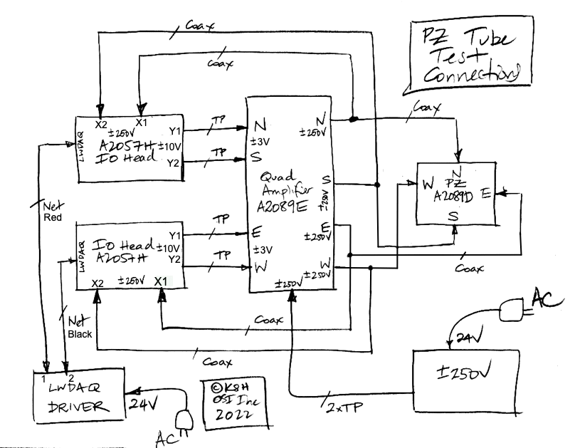
Our ±250 V power supply is a modified A2089C. We could also use our Static Piezo Driver (A2089A), which allows us to adjust the power supply voltages from 0-250 V.
These Y1 and Y2 outputs have dynamic range ±10V, but the amplifiers have a gain of around 80 V/V, so they saturate with input ±3.1V. One eight-bit DAC count is 20/256 = 80 mV at the Y output and later 6 V at the output of the slow amplifier. If we drop the gain of the amplifiers to 25, each count will be only 2 V. Or we could reduce the dynamic range of Y to ±3 V to achieve the same resolution in peizo tube electrode voltage.