Figure: A Four-Pole Active Low-Pass Filter. The dual op-amp provides two stages, each stage generating two poles of the response. For a schematic, see S2071_8.
This guide attempts to teach the design and implementation of active and passive filter circuits through discussion of actual circuits built and used by BNDHEP and OSI. Our discussion begins with high-pass and low-pass filters. We study active implementations, which work well at low frequencies, and passive implementations, which work well at high frequencies. We consider matching networks, which are important at high frequencies for matching sources and loads. We discuss surface acoustic wave filters, which provide astounding performance in a small package. In every case we restrict our discussion to circuits we have built and used ourselves. Transmission lines are a form of filter, but we discuss these separately and in detail in Transmission Line Analysis.
If you are new to capacitors, inductors, and resistors, we introduce these components in the first three lectures of our Introduction to Electronics course. We can always derive the behavior of a filter made of capacitors, inductors, and resistors using differential equations alone. But if we make use of the method of complex impedances, we can derive its frequency response far more quickly than by differential equations. And if we use the Laplace transform, we can derive the frequency response, step response, and impulse response with equal ease. In each of the derivations below, we pick one of these three methods. In our section on pulse shapers, for example, we the impulse response of a filter without the help of the Laplace transform, just to show how it can be done.
Our Filter Tool is a spreadsheet that calculates and plots the frequency response of a variety of filters. We have two versions of the spreadsheet: Filter.ods is for Open Office and Filter.xls is for Microsoft Excel. We use Open Office to create the spreadsheet, so the Open Office version will be more reliable.
An active filter contains an amplifier whose output is connected to its input through passive components, usually capacitors and resistors. This feedback of the output to the input allows us to build filters with imaginary poles using capacitors and resistors alone. Without feedback, a filter with imaginary poles must have both inductors and capacitors. The main purpose of active filters is to eliminate inductors and decrease the value of the filter's capacitors.
In a classic, passive filter made of inductors, capacitors, and resistors, the filter's frequency response is the result of the impedance of inductors and capacitors changing with respect to one another, and with respect to the resistors in the filter. At the cut-off frequency of a filter, the impedances of all its elements will be of the same order of magnitude. Suppose the resistors are of order 1 kΩ, then the inductors and capacitors will have impedance of around 1 kΩ as well. If the filter's cut-off frequency is 1 kHz, the inductors will be of order 100 mH. They might be 30 mH or 300 mH, but not much less or more than that. The RL622-104K-RC is a 100 mH inductor. It is a through-hole part 11 mm high and 8 mm wide that sells for around 50¢. Suppose we drop the resistors to 10 Ω. Now the inductors will be of order 1 mH. We could use the 1812R-105J which is a surface-mount part 4 mm long. They sell for around $1. By reducing the values of the resistors, we reduce the inductors, which is a good thing, but we also increase the capacitors. A capacitor with impedance 10 Ω at 1 kHz would be of order 10 μF. We can get a 10-μF surface-mount capacitor for around 20¢. Now we can drive the circuit with a 1-kHz, 1-V sine wave. Because the resistors are of order 10 Ω, we will draw of order 100 mA from our voltage source. So we could decrease the size of the signal to around 10 mV, and now we draw only 1 mA. Now we must consider another problem: that of the precision of the components. In a 4-pole filter, the component values need to be accurate to within 5% or else the poles will be wrong, and the filter response will not be sharp. If we have to drop the frequency of the filter to 100 Hz, our cost increases tenfold, not to mention its size.
With the help of feedback around low-cost, low-power operational amplifiers (op-amps), we can eliminate inductors and use the same capacitance throughout our filter. If we use capacitors from the same reel of parts, their values are similar. It is the relative values of the capacitors that is most important to the filter response shape. We use resistors of different values, but precise resistors are inexpensive compared to precise capacitors. It is hard to find a 1% accurate capacitor, but a 1% accurate resistor costs only a few cents. If we want to change the filter function, we just buy new resistors. With the help of our Filter Tool, we can try out different resistor values and see what the response will look like. The result is a compact and versatile filter with a precise response. Here is an example 150-Hz low-pass filter that occupies 10-mm square area on one side of a printed circuit board, and consumes less than 5 μA, all for under $5. We discuss operating frequency below, but let us begin with an overview of how operating frequency affects your choice of filter implementation.
At frequencies below 1 kHz, it is almost always better to use an active filter, because at these low frequencies, the inductors required by a passive filter are large and expensive, while low-frequency op-amps are inexpensive and small. Between 1 kHz and 10 MHz, we might use an active filter, or we might use a passive filter made of inductors and capacitors. It depends upon the amount of power we can provide to the active filter's amplifier. The more power we can provide, the faster the selection of amplifiers we can choose from, and the higher the frequency at which the active filter will be effective. These days, for a budget of 10 mA, you can build an active low-pass filter with cut-off frequency 10 MHz. In this schematic you will find a 1.6-MHz four-pole low-pass filter. After reading the sections below, you will know how to enter the gain and time constants of the filter stages into our filter tool, and see the filter's response for yourself.
At frequencies up to 100 kHz, you have a choice of active filter implementation: you can build them with op-amps, capacitors, and resistors, or you can use programmable analog circuits like Lattice Semiconductor's PAC series of chips.
At frequencies above 10 MHz, inductors are small and inexpensive, while op-amps are no longer fast enough to implement filter functions efficiently. Aside from classic inductor-capacitor (LC) filters, like those we buy from Minicircuits, you can get ceramic filters, surface acoustic wave (SAW) filters, and crystal filters. A SAW bandpass filter at 900 MHz costs only a few dollars, and has a response as sharp as a ten-pole LC band-pass filter.
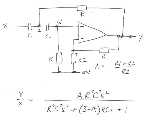
There are many low-pass active filter circuits. We use the one shown in the figure below. As you can see, the output of an op-amp is fed back to its positive input by a capacitor. This capacitor acts as an inductor in the circuit equations. The output is also fed back to the negative input by a resistor divider, and this division gives the active filter its gain, A.

In the Laplace domain, the circuit above has a transfer functions with two imaginary poles. We derive the transfer function below. In the Laplace domain, the ratio of voltage to current for a resistor is R, for a capacitor is 1/sC, and for an inductor is sL. We denote the Laplace transform of the voltage at point X with the letter X, and so on. We obtain the complex gain of the circuit for sinusoidal inputs by replacing the Laplace variable, s, in the transfer function with jω, where j = √(−1) and ω is the angular frequency of a sinusoidal input to the filter.
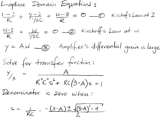
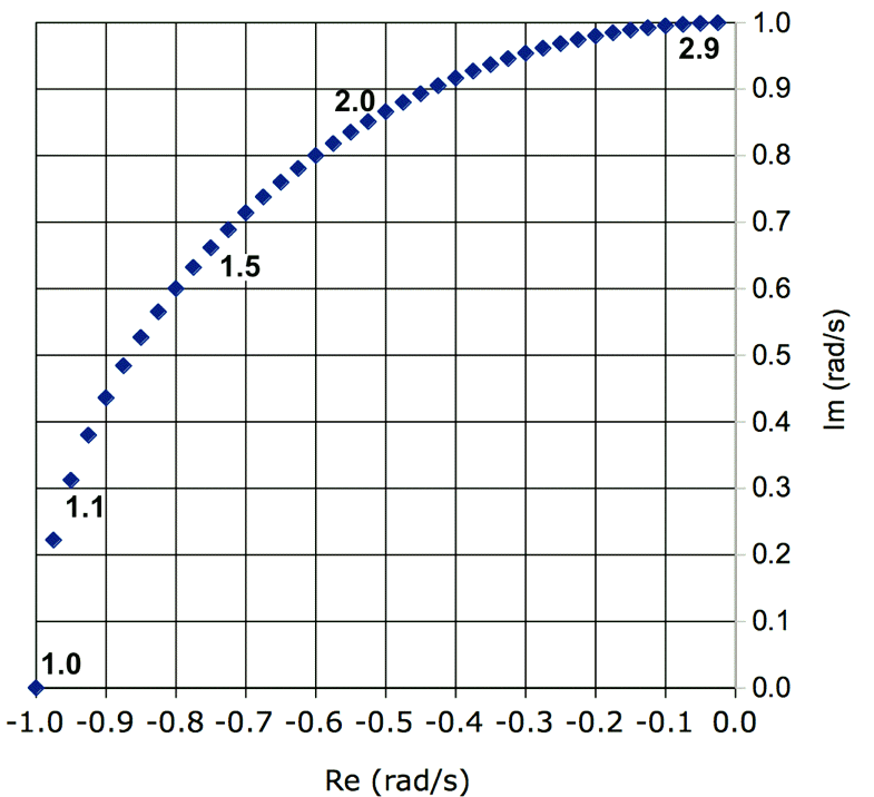
As we vary A, while leaving RC constant, the poles of its transfer function move off the negative real axis of the s-plane, and along the circumference of a circle to the imaginary axis. The radius of this circle is 1/RC, and its center is the origin. The figure below shows the circle's upper-left quadrant.
A Butterworth filter is the filter with maximally flat amplitude response in its pass-band. By cut-off frequency we mean the frequency at which the Butterworth filter output drops to 71% (1/√2) of its maximum amplitude at lower frequencies. The Butterworth filter's maximum amplitude occurs at 0 rad/s, but the Chebyshev filter's maximum amplitude occurs at several other frequencies below the cut-off frequency.
It so happens that the poles of a Butterworth low-pass filter with cut-off frequency ωc are evenly-spaced around the circumference of a half-circle of radius ωc centered upon the origin of the s-plane. The poles of a two-pole filter are at ±45°. Those of a four-pole filter are at ±22.5° and ±67.5°. The following table gives the poles of the low-pass Butterworth filters with one to eight poles and cut-off frequency 1 rad/s. These are called the poles of the normalized Butterworth polynomials.
| Order | Poles |
|---|---|
| 1 | −1 ± j 0 |
| 2 | −0.707 ± j 0.707 |
| 3 | −1 ± j 0, −0.5 ± j 0.866 |
| 4 | −0.924 ± j 0.383, −0.383 ± j 0.924 |
| 5 | −1 ± j 0, −0.809 ± j 0.588, −0.309 ± j 0.951 |
| 6 | −0.966 ± j 0.259, −0.707 ± j 0.707, −0.259 ± j 0.966 |
| 7 | −1 ± j 0, −0.901 ± j 0.434, −0.624 ± j 0.782, −0.222 ± j 0.975 |
| 8 | −0.981 ± j 0.195, −0.832 ± j 0.556, −0.556 ± j 0.832, −0.195 ± j 0.981 |
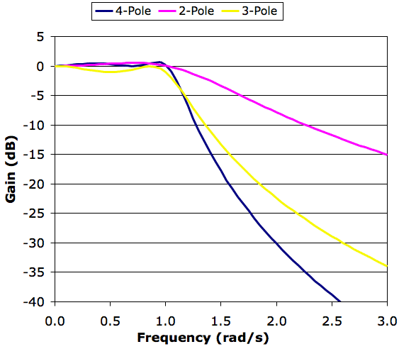
Turn to the Two-Pole LPF, Three-Pole LPF, and Four-Pole LPF sheets in our Filter Tool and you will see places where you can enter the poles of two, three, and four-pole filters. You specify a conjugate pair of poles by giving its real part and the absolute value of its imaginary part. You specify a solitary pole in the three-pole filter by giving its real part only. We provide a table of example pole sets for various filter functions. As you enter new pole values, the Filter Tool plots the amplitude response of your poles.
We implement each conjugate pair of poles with a single op-amp stage, as shown above. We can implement solitary poles with an RC network, or in another op-amp stage with a capacitor across its feedback resistor. This single-pole op-amp stage allows us to amplify and filter at the same time. With two op-amps we can implement a three-pole low-pass filter with amplification. In this circuit, you see a three-pole filter made out of two op-amps. It has a 10-MΩ input resistance with a 0.15-Hz high-pass filter, followed by a three-pole filter, and provides a total gain of 25. We implement the single pole with a capacitor across the first op-amp's feedback resistor. At high frequencies, the capacitor reduces the ×11 gain of the first op-amp stage to ×1. Ideally, the capacitor should reduce the gain to ×0, which it would if we arranged the op-amp as an inverting amplifier. But a reduction in gain from ×11 to ×1 is a good enough approximation for our filter to work well.
The frequency plot extends from 0 rad/s to 3 rad/s. The plot is intended for use with the poles of normalized filter polynomials, which are polynomials whose cut-off frequency is 1 rad/s. If we want to make a 4-pole Butterworth low-pass filter with cut-off frequency ωc using active filter stages like the one shown above, we build two stages, each with RC=1/ωc, and pick the value of A of each stage to put its two conjugate poles at the correct place on the circuit of radius ωc in the s-plane. These values of A are independent of ωc, so we can look at the Pole Locus figure and the Normalized Poles table above, and figure out the gain we need to produce the poles of the normalized Butterworth filter. We use these values of A in our filter with cut-off frequency ωc. You can determine A with sufficient accuracy by interpolating between points in the pole locus, knowing that these points represent steps of 0.1 in A, starting with 1.0 with the two poles together on the negative real axis.
Instead of using the pole locus to determine the correct values of A for your Butterworth filter stages, select the Pole Locus sheet in our Filter Tool. There you will find the data for our pole locus figure, and a place where you can enter values of A and RC, and get the pole real and imaginary parts of the resulting conjugate pole pair. We have done this for you, and present the correct values of A in the table below. Note that filters with an odd number of poles require only an R-C network to implement the solitary pole on the negative real axis. In case you are wondering: the ordering of the stages is not important. The filter will work just as well with any sequence of correct gain values.
| Filter Order | Gain Values (A in V/V) | Total Gain (V/V) |
|---|---|---|
| 1 | 1* | 1.0 |
| 2 | 1.59 | 1.6 |
| 3 | 1*, 2.00 | 2.0 |
| 4 | 1.15, 2.24 | 2.6 |
| 5 | 1*, 1.38, 2.38 | 3.3 |
| 6 | 1.07, 1.59, 2.48 | 3.9 |
| 7 | 1*, 1.20, 1.75, 2.56 | 5.4 |
| 8 | 1.04, 1.34, 1.89, 2.61 | 6.9 |
On page five of our Filter Tool you will see how you can vary A and RC of one-stage, one-and-a-half stage, and two-stage active filter to create a two-, three-, and four-pole low-pass filters. If you set RC to 1, and enter the Butterworth values of A from the table above, you will see the Butterworth maximally flat amplitude response, with cut-off frequency 1 rad/s (0.16 Hz). All stages of a Butterworth filter have RC=1/ωc, where ωc is the cut-off frequency in rad/s. We have fc = ω/2π the cut-off frequency in Hertz. Vary RC for each stage by a factor of two or so, as well as varying A, and you will obtain a variety of other responses, especially with the two-stage filter. We provide RC and A values for ωc = 1 rad/s. Try the Chebyshev 0.5-dB ripple response, which we show below.
If you want to build a filter with a response of the same shape as the one you see above, but with cut-off frequency ωc, divide each stage's RC by ωc, but leave A the same. You will now have the same response shape, but with the frequency axis scaled by ωc. You can experiment with values of A and RC in the Active LPF sheet of our Filter Tool to see what the resulting filter response looks like. You will find that trying to obtain the Chebyshev 3-dB Ripple response by trial and error is difficult. That's why we tend to use tables of pre-calculated poles to build our filters. For the poles of a variety of Chebyshev filters, look here.
| A2071 | 10.6 kHz Four-Pole Anti-Aliasing Filter (U20) |
| A2065 | 1-kHz Four-Pole Square to Sine Converter (U7) |
| A3006 | 160-Hz Four-Pole Anti-Aliasing Filter (U6) |
| A3008 | 1.5-MHz Four-Pole Intermediate Frequency Filter (U8) |
| A3028 | 160-Hz Three-Pole Anti-Aliasing Filters (U5 and U6) |
| Rough | 10-kHz Four-Pole Modulation Rejection Filter |
The above table gives some example low-pass filters. You can plot the frequency response of each filter using the Active LPF page of our Filter Tool. Calculate the gain of each op-amp stage, enter it into the corresponding gain cells. Calculate RC for each stage. Multiply all the RC values by the same scaling factor so that they are all of order 1 s. Enter the scaled RC values into the corresponding time constant cells. You will see the filter response plotted as you make your changes.
You can change the low-pass filter into a high-pass filter by exchanging the resistors and capacitors, as show below. The poles of the transfer function remain fixed, but we introduce two zeros at the origin.
As we can see from its transfer function, the high-pass filter is equivalent to a double-differentiator in series with the same low-pass filter we would have obtained with the same resistor and capacitor values. At high frequencies, the amplification of the double-differentiator is cancelled by the attenuation of the low-pass filter, giving us flat response. At low frequencies, the attenuation of the double-differentiator is dominant, and causes a reduction in the output amplitude with decreasing frequency. When the angular frequency of the input, ω, is equal to 1/RC, the response of the high-pass filter and the low-pass filter are equal. Another way of considering the transfer function is to say that the high-pass filter response is the low-pass filter response subjected to the transformation RCs = 1/RCs', so that the response of the high-pass filter at angular frequency 1/RC equals that of the low-pass filter at the same frequency, and at angular frequency 2/RC it equals that of the low-pass filter at frequency 1/2RC.
You will find a poor drawing of a 19-kHz two-pole Butterworth high-pass filter here, along with accompanying calculations. The capacitors are 4.7 nF, R is 1.8 kΩ, and A = 1.59.
Filters made with passive components get larger and heavier as their cut-off frequency decreases. A 10-kHz high-pass filter made with inductors and capacitors, feeding a 50-Ω load, must contain inductors whose impedance is of order 50 / 2π.10kHz ≈ 1 mH. A 1-mH inductor with series resistance less than 5 Ω (10% of 50 Ω) is hard to find for less than $5, and it will be at least 15 mm on each side. A capacitor with impedance 50 Ω at 10 kHz is roughly 330 μF. Capacitors that size tend to be electrolytic, and therefore polarized, so that you can't connect them to an alternating voltage. By the time we get down to 100 Hz, the inductors and capacitors are huge, and we tend to see them used these days only for filtering power supplies.
Passive filters are cumbersome at low frequencies, but active filters stop working at high frequencies. The amplifier in most active filters is an operational amplifier, or op-amp. Op-amps are high-gain differential amplifiers with a negative and positive input. They have their own internal gain, which is large at low frequencies, but drops as frequency increases. Most op-amps have internal compensation, which means they have a capacitor somewhere inside that acts as a single-pole low-pass filter in series with their large gain. Without this compensation, op-amps tend to be unstable in feedback loops, and designers don't like to worry about instability in op-amp circuits. Even without the capacitor, the op-amp gain drops with frequency, but it does so in an irregular and unpredictable way.
Because of the compensating capacitor, the gain of an op-amp feedback amplifier is inversely proportional to its half-power bandwidth, and so we have the gain-bandwidth product of an op-amp, which is the product of the gain of any feedback amplifier you make out of the op-amp and the frequency at which loss of op-amp internal gain causes a 29% (3 dB) drop in output amplitude.
Suppose the gain-bandwidth product of our op-amp is 1 MHz, which is the case for the OPA2277 we use in this filter. The second stage of the filter has gain 2.27, so its bandwidth is 1 MHz / 2.27 ≈ 400 kHz. The cut-off frequency of the filter, fc is 10 kHz. The amplifier bandwidth is forty times greater than the cut-off frequency. Our rule of thumb is that the amplifier bandwidth should be at least ten times greater than the filter cut-off frequency. With stage gains of around two (2), the OPA2277 allows us to build filters with cut-off frequencies up to 40 kHz.
Another of our favorite op-amps, the LM6172, has gain-bandwidth product 100 MHz, and would support filters with cut-off frequency up to 10 MHz. At higher frequencies, there's not much point in using an active filter, because inductors are simpler (provided that you know how to design passive filters). Consider a passive 10-MHz low-pass filter driven by a 50-Ω source, and terminated by a 50-Ω load. The inductors in the filter should have impedance comparable to 50 Ω at 10 MHz, which means their inductance, L, should be of order 50 / 2π.10MHz ≈ 1 μH. We can buy a 1-μH inductor in a P0805 surface-mount package with series resistance less than 0.2 Ω and self-resonant frequency 100 MHz for less than ten cents. The filter won't work so well at 1000 MHz, because the parasitic capacitance of the cheap inductor will be passing the 1000 MHz through the filter, but you can block frequencies ten times higher than the cut-off with an auxiliary single-pole low-pass filter with cut-off frequency 100 MHz. You can make that filter out of a capacitor and a resistor. You can find tables of inductor and capacitor value for normalized filters on the web. A table for low-pass Chebyshev filters is here
Programmable analog circuits, such as those provided by Maxim Semiconductor and Lattice Semiconductor, use analog switches and capacitors to make switched capacitor filters. By connecting a capacitor to two terminals only 10% of the time, you create a capacitor 10% as large. The speed of these circuits is limited by the capacitor switching frequency. The latest circuits appear to support switching frequencies up to 1 MHz, which means we can use them to make filters that operate up to about 100 kHz.
Speaking for ourselves, we use active filters below 1 MHz, passive filters above 10 MHz, and debate with ourselves for the range in between. We have not yet seen a need for programmable filters, but when we do, we look forward to using them at frequencies below 100 kHz.
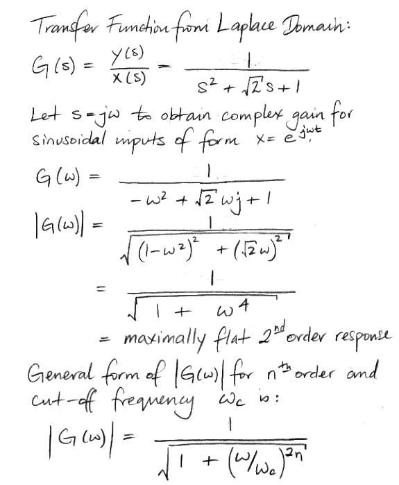
By varying the poles of the four-pole filter on the second page of our Filter Tool, you will see how sensitive the response is to the pole values. The Butterworth Polynomials provide us with maximally flat amplitude response in the pass-band. The ratio of the output amplitude to the input amplitude is (1 + ω2n/ωc2n)-½, where n is the number of poles in the filter, ω is the frequency of the input in rad/s, and ωc is the cut-off frequency in rad/s. This amplitude relation defines the Butterworth Polynomials. The figure below shows how the normalized second-order Butterworth Polynomial, s2 + s√2 + 1, provides the specified frequency response. The normalized polynomial is the polynomial for ωc = 1 rad/s. The poles of this normalized second-order polynomial are the poles we give in row two of the table above.
The Chebyshev Polynomials provide us with the Chebyshev filter poles. The Chebyshev polynomials allow you to accept variation in the pass-band amplitude response in exchange for sharper cut-off just outside the pass band. The normalized second-order Butterworth amplitude response reduces to (1 + ω4)−½. There is no term in ω2. Because there are no term in ω2, the amplitude response is always decreasing as frequency increases, and contains no ripples. But if we can accept some ripples in the pass-band amplitude response, then we can add an ω2 term that cooperates with the ω4 term to drop the response more sharply above ωc.
You can see the basis of the Chebyshev polynomial derivation here, and we give you the the normalized 3-dB passband ripple Chebyshev polynomials in the table below, where you can compare them to the normalized Butterworth polynomials.
| Filter Order | Chebyshev, 3-dB Ripple | Butterworth |
|---|---|---|
| 1 | s + 1 | s + 1 |
| 2 | 1.41s2 + 0.911s + 1 | s2 + 1.41s + 1 |
| 3 | 3.98s3 + 2.38s2 + 3.70s + 1 | s3 + 2.00s2 + 2.00s + 1 |
| 4 | 5.65s4 + 3.29s3 + 6.60s2 + 2.29s + 1 | s4 + 2.61s3 + 3.41s2 + 2.61s + 1 |
| 5 | 15.9s5 + 9.11s4 + 22.5s3 + 8.71s2 + 6.48s + 1 | s5 + 3.24s4 + 5.24s3 + 5.24s2 + 3.24s + 1 |
All the polynomials in the table above have value 1 for s = 0. If our transfer function has the polynomial in its denominator, its gain for ω = 0 rad/s will be 1. At ω = 1 rad/s, all the polynomials produce a gain 3-dB less than the maximum gain for ω ≤ 1 rad/s. The maximum gain of the Butterworth filter is 1, and occurs at ω = 0 rad/s, but the maximum gain of the 3-dB Chebyshev filter is √2, or 3 dB greater than unity, and occurs at one or more values of ω between 0 rad/s and 1 rad/s. The gain of the Chebyshev filter at ω = 1 rad/s is 1.
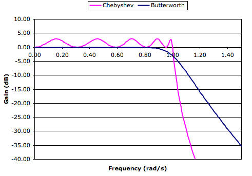
By comparing the Chebyshev and Butterworth polynomials, you can see why the Chebyshev provides a sharper cut-off outside its pass-band. The s5 term in the fifth-order Chebyshev polynomial has coefficient 15.9, while the s5 term in the Butterworth polynomial has coefficient 1. For frequencies less than ωc, the fifth-order Chebyshev polynomial balances its large s5 term with large s4, s3, s2, and s terms. This balancing is done in such a way that we produce the minimum amount of ripple in the pass-band response for the maximum coefficient in s5. Once ω rises above ωc, the s5 term overtakes all other terms rapidly, and gives a sudden drop in response. Not only does the Chebyshev filter always give us a sharper cut-off than the Butterworth filter, but the advantage grows with the order of the filter, as you can see in the graph above.
A passive filter is one made up of inductors, capacitors, and resistors. In most cases, the only resistors in the filter are the source and load impedances. These resistors might exist in your circuit as separate resistor components, or they might be an inherent feature of the amplifier that provides the signal and the amplifier that receives the output of the filter. In the section above on filter polynomials we show how you arrive at a polynomial function of frequency that best matches your requirements. Passive filters implement these polynomial frequency responses with capacitors and inductors that interact with your source and load impedances.
We will present an example passive filter design later in this section, but we begin with a quantitative introduction to the subject. One way to start off learning about passive filters is to use a passive filter calculator like this one. You enter your source and load resistances, pick a classic polynomial frequency response (Butterworth, Chebyshev, Bessel, as described above), pick the order of the polynomial (the highest power of frequency in the transfer function), and a characteristic frequency for the response, such as the −3 dB point for a Butterworth low-pass or high-pass filter. The calculator gives you a circuit diagram and gives you the inductor (L) and capacitor (C) values in Henries (H) and Farads (F).
A classic passive filter, such as the ones designed by the calculator linked to above, takes the form of a sideways ladder, in which the bottom rail is a signal ground, and the top rail is a series of inductors or a series of capacitors. It will be inductors in a low-pass filter and capacitors in a high-pass filter. The steps of the ladder (if the ladder were vertical they would be the steps) are capacitors in a low-pass filter and inductors in a high-pass filter. The total number of capacitors and inductors in the ladder is equal to the highest power of frequency in the frequency polynomial, and gives us the order of the filter. The ladder is the favored structure for passive filters because the method of continued fractions allows us to convert a polynomial frequency function into a ladder circuit with comparative ease.
Given that the filter is a ladder, another thing you need to specify for a passive filter is whether it is a "shunt" or "series" filter. A shunt filter is one in which the first element connects to signal ground (0 V). A series filter is one in which the first element connects to the second element, and the second element connects to ground.
If your source impedance is zero, a shunt filter does not make sense, because no component to ground can affect a signal with zero source impedance. But zero source impedance is in any case impractical when driving a passive filter. The impedance of the filter, as seen by the source, tends to drop dramatically near the cut-off frequency, regardless of whether it is a shunt or series arrangement. When the filter impedance drops, the current drawn from the source will increase dramatically until the source can no longer maintain the appearance of zero source impedance, and the input signal becomes severely distorted. Thus the performance of the filter is compromised in practice when we design for zero source impedance. A finite source impedance reduces the current the filter must draw, at the expense of losing some signal amplitude. But we assume that this amplitude can be made up later with an amplifier.
Infinite load impedance turns out to be impractical also, because it requires infinite-valued inductors and infinitesimal capacitors. Indeed, any time the ratio of the source to load impedance is greater than ten, the filter is going to be hard to build with standard parts.
When you are thinking about these passive filter circuits, and how they interact with your amplifiers, keep in mind that a voltage source, V, in series with a resistor, R, is equivalent to a current source I = V/R in parallel with the same resistance, R. If your signal source is the collector of an NPN transistor driving a 50 Ω load, the collector is equivalent to a voltage source in series with this resistor. You can shunt the output to ground through a capacitor to start a low-pass filter, or you can put an inductor in series with it. On the other hand, you cannot shunt it to ground with an inductor to start a high-pass filter because you will ruin the DC bias of the transistor. But you could start with a large series capacitance, whose impedance is negligible compared to the source impedance, to isolate the transistor from the filter at DC, and then begin your high-pass filter with an inductive shunt to ground.
In all cases, and throughout the filter, you will find that the impedance of each individual capacitor and inductor is of the same order as the source and load impedances at your desired high-pass or low-pass cut-off frequency. If your source impedance is 50 Ω and your load impedance is 500 Ω, the impedance of the components will increase from through the circuit so that those closest to the source are of order 50 Ω, and those closest to the load are of order 500 Ω.
You are likely to be using active filters in the cases where you have high source and load impedances, or mismatched impedances. Your most likely application for a passive filter will be in radio-frequency circuits where amplifiers have 50 Ω output and input impedance. But there are other times when a passive filter is the simplest and most compact solution, and we will study one as an example.
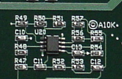
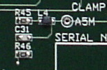
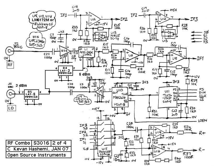
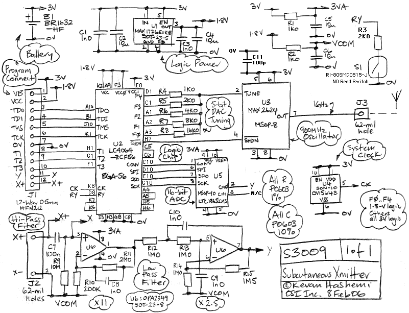
Consider the anti-aliasing filter consisting of R45, L4, C31, and R46 in S2071_8. The photograph below shows what this circuit looks like, made out of 0805 surface mount components.
We re-draw the circuit diagram below, with the component names changed. This filter provides a 5-MHz pass-band with attenuation of 20 dB at 20 MHz in order to prepare the signal VR for digitization at 40 MSPS. A two-pole maximally flat Butterworth response is adequate. Resistor R1 inserts a source impedance into the signal path. Without this, L and C will present a near-zero impedance near their natural resonant frequency 1/(2π√(LC)), and this will over-load op-amp that provides the input X. We choose R1 = 100 Ω to limit the input current to 5 mA for a 0.5-V applied signal.
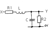
Resistor R2 provides a finite load impedance. The larger the load impedance in comparison to the source impedance, the less the filter will attenuate frequencies within its pass band. If we chose R2 = 100 Ω, our output would be half the amplitude of our input. We would our filter to attenuate the signal as little as possible, so we want to choose a load impedance much larger than the source impedance. The higher the load impedance, however, the larger the value of L required to generate a comparable impedance at 5 MHz. We choose R2 = 1 kΩ. At low frequencies the filter attenuation will be 1 dB, which is slight. The amplifier to which we connect Y must have an input impedance much greater than 1 kΩ, or else it will affect the performance of the filter. An input impedance much higher than 1 kΩ is easy to achieve with another op-amp.
We now calculate the gain and phase shift of this circuit for sinusoidal inputs. We let the impedance of a capacitor be 1/sC, the impedance of the inductor is sL and that of the resistor is R. Here we are using s for the Laplace variable. The transfer function of the filter is the ratio of the impedance from point Y to 0 V divided by the impedance from X to 0 V through the filter. If we were to use the complex exponential to obtain the gain and phase, we would follow the same procedure, but with the impedances set to 1/jωC, jωL, and R, where j = √(−1) and ω is angular frequency. In the calculations below, we determine L and C for the maximally-flat low-pass response with cut-off frequency 5 MHz.
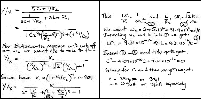
The first time we performed the above calculation, in our notebook, we lost the factor of √2 required for the maximally flat response, and concluded that 270 pF and 3.3 μH were correct. We built the filter with these values, applied a sinusoid to the input, and measured the input and output amplitude while increasing the frequency. We obtained the following plot of gain versus frequency.
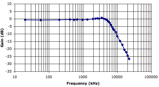
If we take the cut-off frequency as the point at which the attenuation drops 3 dB below the pass-band, we see the actual cut-off frequency of our filter is around 6 MHz. Instead of maximally flat response in the pass-band, we have a 1-dB ripple just before the cut-off. So far as we are concerned, this response is close enough to the one we wanted.
Instead of building a filter that acts upon an input voltage to produce an output voltage, we can sample the input voltage at regular intervals, digitize the samples, and perform the filtering in a microprocessor. We sample the input voltage at the sampling frequency, which we denote fs = 1/Ts. After sampling and digitization, the input voltage, X(t), becomes a sequence of binary values Xn = X(nTs). At each sample instant, we calculate the filter output, Yi. If necessary, we translate Yi into a sequence of voltages Y(nT). The output voltage is equal to Y(nT) for time nT ≤ t < (n+1)T. The initial digitization of X will produce an integer value. But subsequent calculations may take place in integer arithmetic, floating point arithmetic, or integer fraction arithmetic.
A recursive filter is one that calculates Yi as a linear sum of the present and past values of the input samples, and of the past values of the output samples themselves. Thus the filter operates not only upon its input, but refers to the history of its own output as well. In general, the impulse response of a recursive filter lasts forever, even as it becomes vanishingly small. The following equation gives the general form of a recursive filter.
Yi = a0Xi + a1Xi-1 + a2Xi-2 + ... +adXi-d + b1Yi-1 + b2Yi-2 + ... + bdYi-d
Here d is the depth of the filter, which is how many samples of X and Y we have to keep on hand in order to calculate the filter output. To implement a filter of depth d we have to store 2d values. The filter also requires that we have on hand 2d + 1 constants for calculating the linear sum.
If we want to use a recursive filter to implement a low-pass, high-pass, or band-pass frequency response, we must have some way of determine its frequency response from its filter constants. One way to determine its frequency response is to implement it in software, apply sinusoids of increasing frequency, and calculate the amplitude of the output for each frequency. But there is a simpler way. We express the filter as a transfer function with the help of the z-transform and the complex exponential. The z-transform allows us to represent a delay of Ts as z−1. Instead of writing Xi-1 we write Xz−1. The formula above becomes:
Y = a0X + a1Xz−1 + a2Xz−2 + ... +adXz−d + b1Yz−1 + b2Yz−2 + ... + bdYz−d
= (a0 + a1z−1 + a2z−2 + ... +adz−d) X + (b1z−1 + b2z−2 + ... + bdz−d) YAnd from the above we can obtain the transfer function of the recursive filter in the z-domain.
Y/X = (a0 + a1z−1 + a2z−2 + ... +adz−d) / (1 − b1z−1 − b2z−2 − ... − bdz−d)
We now note that because z−1 is a delay of Ts, the effect of multiplying a sinusoid of angular frequency ω by z−1 is the same as a phase delay of ωTs. The effect of multiplying by z is the same as a phase advance of ωTs. If we represent X with the complex exponential e jωt, the effect of multiplying X by z is the same as multiplying X by e jωTs. We let z = e jωTs in the above transfer function to obtain the sinusoidal gain of the filter.
Y/X = (a0 + a1 e−jωTs + a2 e−2jωTs + ... +ad e−djωTs) / (1 − b1 e−jωTs − b2 e−2jωTs − ... − bd e−djωTs)
For example, consider the following recursive filter:
Yi = 0.125 Xi + 0.875 Yi-1
Using the z-transform, the transfer function of this filter is:
Y/X = 0.125 / (1 − 0.875z−1)
Its sinusoidal gain at angular frequency ω is:
Y/X = 0.125 / (1 − 0.875 e−jωTs)
When ω = 0, e−jωTs = 1 and the filter gain is 1. When ω = π/Ts, which is the same as saying the frequency of the sinusoid is half the sampling frequency, e−jωTs = −1 and the filter gain is 0.067. When ω = 2π/Ts, so our sinusoid has the same frequency as the sampling frequency, e−jωTs = 1 and the gain is 1. In general, the gain at frequency ω < π/Ts is the same as the gain at frequency 2π/Ts−ω. Which is to say: the gain at sinusoidal frequency f < fs/2 is the same as the gain at frequency fs−f. So, if we consider only frequencies below fs/2, our recursive filter provides a low-pass frequency response. This restriction to frequencies lower than half the sample frequency applies to all recursive filters, and fs/2 is known as the Nyquist frequency.
The following recursive filter provides a high-pass response.
Yi = 0.984375Xi − 0.984375Xi-1 + 0.96875Yi-1
Using the z-transform, the transfer function of this high-pass filter is:
Y/X = (0.984375 − 0.984375z−1) / (1 − 0.96875z−1)
If we multiply its transfer function by that of our low-pass filter, we obtain a band-pass filter transfer function with the following recursive filter representation.
Yi = 0.123046875Xi − 0.123046875Xi-1 + 1.84375Yi-1 − 0.84765625Yi-2
The constants in the low-pass filter were multiples of 1/8. Those in the high-pass filter were multiples of 1/64. Those in the band-pass filter are multiples of 1/512. If we want to implement the band-pass filter with fractions no finer than 1/64, we should do it in two stages rather than one stage.
In the Recursive sheet of our Filter Tool, you can expriment with recursive filters up to depth four, by entering their constants into an array. The Filter Tool uses the z = e jωTs substitution to obtain the gain of recursive filters at various frequencies, and it plots their frequency response as shown below.
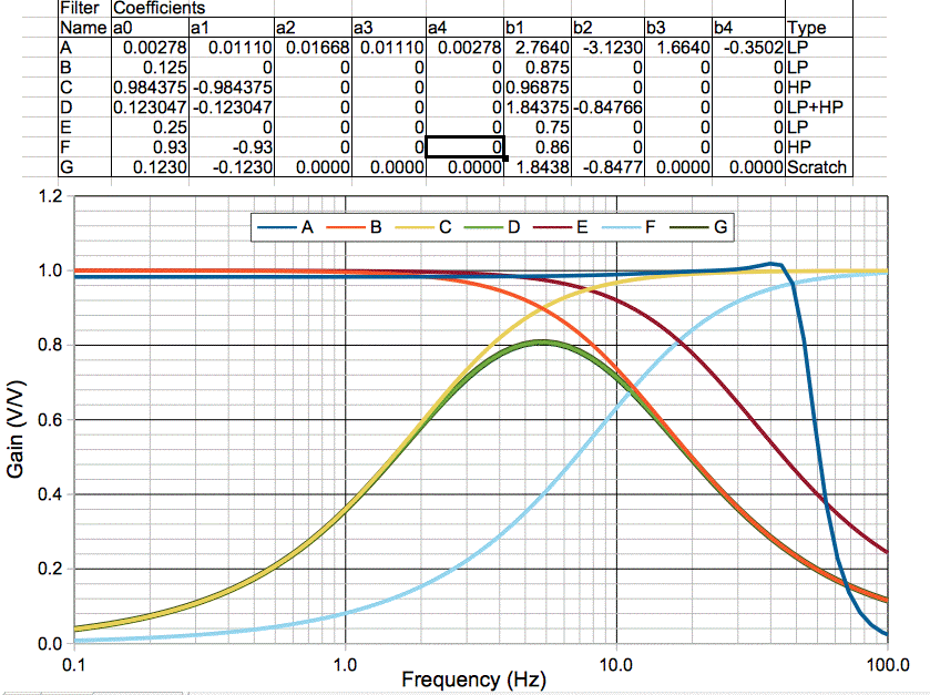
By making small changes to the constants, you will see how sensitive the recursive filter is to the exact values. The constants need to be correct to better than 1% for a filter of depth two, and 0.01% for a filter of depth four.
A matching network is a passive filter that changes the effective impedance of a source or load. We can use a transformer as a matching network. A transformer has a primary and secondary coil both wound around the same core. Suppose the secondary side has N times more turns than the primary. We apply a sinusoidal voltage of amplitude V to the primary coil and we observe amplitude NV on the secondary coil. We attach a resistance R to the secondary coil and observe current NV/R flowing into the resistor in phase with the secondary voltage. The current flowing into the primary coil, meanwhile, is in phase with the applied voltage, and has amplitude N2V/R. The power flowing into the primary coil is N2V/R × V = N2V2/R. The power flowing out of the secondary coil into the resistor is likewise N2V2/R. The source of the primary coil voltage sees a load of R/N2, not R.
Suppose we have a source of radio-frequency power, something like the RFPA3800 transistor, and this source has amplitude 5 V rms and impedance 10 Ω. We want to drive an antenna with impedance 50 Ω. If we connect the two together directly, the amplifier may oscillate. But suppose the amplifier remains stable. It generates 5 V rms and this passes through its 10-Ω output impedance and into the 50-Ω input impedance of the antenna. The antenna will get 350 mW of radio-frequency power. If, instead, we connect the 50-Ω antenna to the secondary side of a transformer with N = √(50/10) = 2.24, the antenna will appear as a 10-Ω load at the amplifier, and will receive 625 mW of power. The voltage on the primary coil will be 2.5 V rms and on the secondary will be 5.6 V rms.
Transformers can match impedances over a wide frequency range. The ADT4-5WT from MiniCircuits operates form 0.3-500 MHz and has impedance matching ratio 4.0 (turn ratio 2.0). When we have space on the board for a transformer, and we want broad-band matching of a resistive source and load, the transformer is a good choice.
But not all loads and sources are purely resistive, and we sometimes prefer our matching networks to be effective only at a certain frequency. Indeed, there are times when we want our matching network to remove signals outside a very narrow frequency range. Sometimes, a capacitor and inductor can perform superb matching and discrimination. We are going to explore these issues by looking at a passive circuit that selects a narrow band of frequencies, and moving on to another passive network that that does the same thing but with amplification and impedance matching at the same time.
The circuit below is the resistor-tank tuning circuit from our Command Receiver (A3023CR). A tank circuit is a capacitor and inductor in parallel. At some frequency, the magnitude of the inductor impedance equals that of the capacitor, but they have opposite phase. Current that flows out of the inductor flows into the capacitor, and visa versa. The voltage on the tank grows until it matches the voltage applied to it, so that no more current can join the exchange between the capacitor and inductor. We call this condition resonance. There is plenty of current flowing between the capacitor and inductor, but from the outside, the impedance of the two in parallel appears to be very large. Indeed, for a perfect inductor and capacitor, their parallel impedance will be infinite at the resonant frequency.
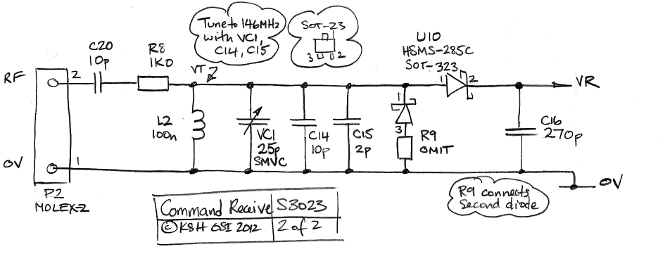
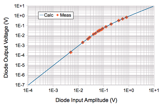
The circuit shows an input for an antenna. Our intention is to pick up 146 MHz power with a couple of loops of stainless steel wire. Capacitor C20 provides low-frequency blocking. The crystal diode, U10, has effective resistance 10 kΩ for radio frequencies (for more about the diode, see here). At the resonance, the impedance of the L2 in parallel with VC1, C14 and C15 is well over 10 kΩ. Resistor R8 and the crystal diode form a voltage divider and we get 90% of the antenna voltage on the diode. The diode provides a DC voltage on C16 that increases with RF power, as in this plot. At other frequencies, the tank circuit has a much lower impedance, and so decreases the amplitude of the signal on the diode. The following traces show the response of the circuit when we set the tank capacitance to 1.0 μF and inductance to 1.0 μH. We expect resonance at f = 1/(2 π √(LC)) = 8 MHz, which is what we get.
The tank tuner gives good frequency selection. But its gain is only 0.9 at the desired frequency. We note that the impedance of the detector diode is 10 kΩ, while the resistance of our antenna is far smaller, which means there is more power available in the antenna than is being delivered to the diode. We estimate the source impedance of our small, steel, loop antenna is 100 Ω in series with 300 nH. Because the source impedance is a hundred times lower than the load impedance, we can hope to amplify the antenna signal with a matching network before presenting it to our detector diode.
The circuit we present below is supposed to represent a small loop antenna, a matching network, and a detector diode. The resistor R2 is the resistance of the antenna wire, which is significant at radio frequencies because of the skin effect. The inductor L1 is the self-inductance of the antenna. The matching network components are C1, R3, L2, and C2. The detector diode is represented by R1, which is its effective resistance at zero bias.
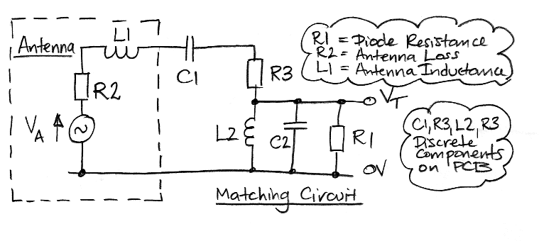
By choosing various values for this circuit, we can model not only our antenna and detector diode arrangement, but many other matching networks besides. The Matching sheet in our Filter Tool plots the frequency response of the network for any combination of values. With R2 = 10 Ω and R1 = 50 Ω, we can experiment with various values for the other components to see if we can match the source to the load impedance. When we want to leave out a component, we pick a large or small value for it that makes its contribution to the activity negligible. Thus we could set L1 to 0 nH to leave it out, or C1 to 10000 pF.
For now, however, let us return to the problem of matching our loop antenna signal to our detector diode. Let us set R3 = 0 Ω, C1 = 1 pF, C2 = 10 pF, and L2 = 100 nH. This arrangement is a spit-capacitor matching network. When compared to the resistor-tank network, it provides dramatically improved performance. We use the split-capacitor matching network in our A3024A miniature, micropower, radio receiver.
In the split capacitor network, the tank circuit resonates at our operating frequency. The voltage, VT, on the tank is almost opposite in phase to the voltage applied to C1 by the antenna. The amplitude of the voltage across the capacitor is almost equal to the sum of the antenna and tank amplitudes. Suppose the antenna amplitude is 100 mV, the tank amplitude is 900 mV, and the small capacitor has reactance 1 kΩ. We have 1.0 mA flowing into the capacitor, which is the same current we would see if we connected a capacitor 10 times as large directly to the 100 mV produced by the antenna. Thus the antenna sees an effective reactance of only 0.1 kΩ, while the tank circuit sees an effective reactance of 0.9 kΩ. This simple consideration shows us how it is possible, with a humble capacitor, to match two differing source and load impedances at a particular frequency.
By inserting jωL for inductors and 1/jωC we can calculate the complex gain of the above circuit, where ω = 2π f is angular frequency and j is √(−1). We arrive at the following solution.
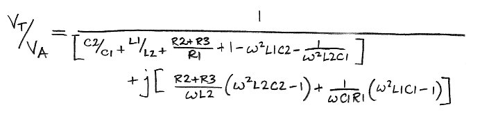
We see that the circuit has four resonant frequencies corresponding to all combinations of the two inductors with the two capacitors. When we are near the resonance of L2 and C2, the gain increases. We calculate the gain using the above formula in the Matching sheet of our Filter Tool, and we plot it below for various component values.
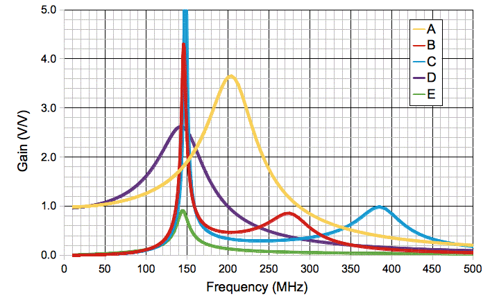
The table below gives the component values that we used to obtain each plot. The values for plot E correspond to our original resistor-tank circuit.
Plot D shows what happens if we match an antenna with self-inductance 300 nH and resistance 100 Ω to a 10-kΩ load with a 4-pF capacitor. We get a nice peak in gain at 146 MHz. Our matching network consists of only one component: a 4-pF capacitor. In general, we can match any two source and load impedances with a single inductor and capacitor. In this case, we are using the antenna self-inductance as the inductor in the matching network. But the antenna self-inductance changes by ten percent or so when we bend it or handle it. Plot A shows the response of the same 4-pF capacitor matching network when the antenna inductance is instead 150 nH and its resistance is instead 50 Ω. The peak in gain moves up to 200 MHz and our matching is no longer effective at 146 MHz.
Plots B and C show the gain generated by a split capacitor network. In both cases, the matching circuit components are the same, but we have changed the antenna inductance and resistance by a factor of two. The peak in gain differs by only a few Megahertz. Changes in the antenna have very little effect upon the primary resonance of the matching network. This insensitivity to the antenna properties is what makes the split-capacitor network robust and effective in practice. There is a secondary resonance also, between the antenna inductance and the matching capacitor. This resonance moves when we change the antenna inductance. But it is not the resonance we are relying upon to provide matching gain.
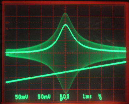
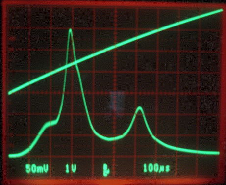
Here is the response of an actual split-capacitor matching circuit as we sweep the antenna frequency through 116-198 MHz. We have C1 = 1 pF, C2 = 8 pF, L2 = 100 nH and R3 = 0 Ω. The trace with two peaks is the output of our detector diode, and so is not directly proportional to the gain of our matching network, but nevertheless increases with gain. The first peak corresponds to gain 4.5 at 146 MHz and the second to gain 2.5 at 170 MHz. We see that our antenna signal is being amplified for our detector diode by the action of purely passive components.
When we insert these component values into our Filter Tool, along with our estimate of antenna resistance and inductance, our calculation suggests the first peak should be at 160 MHz with gain 4.6 and the second should be at 310 MHz with gain 0.9. Thus our calculation captures the spirit of the matching network's behavior, but in reality the layout of the printed circuit board, imperfections in the individual components, and uncertainty about the antenna, require that we select the tuning capacitance during construction. This is often the case with matching networks. If we want such spectacular performance by a passive network, we will have to adjust the circuit at the time of construction.
We can use matching networks on the output of amplifiers also, so as to match their output impedance to that of our load. In our Command Transmitter (A3029A) Manual, you will find a record of our measurements of the reflection coefficient of the input and output of an amplifier, and subsequent calculation of the correct matching impedance to provide efficient delivery of power from and to 50-Ω loads.
When a photomultipliers detects the flash of light generated by a subatomic particle, it generates a voltage pulse ten or twenty nanoseconds long. The area of this voltage pulse is proportional to the intensity of the flash of light. To make use of the photomultiplier output, we must measure the area of the pulse. The simplest method is to digitize the pulse at 1 GSPS, and so obtain 20 samples of a 20-ns pulse and calculate its area in a computer. But sampling at 1 GSPS is hard to do, and wasteful if the flashes of light are rare. Another method is to integrate the pulse with a transistor and a capacitor, digitize the final value of the integrator when the pulse is complete, then reset the integrate in readiness for the next pulse. Another method, which turns out to be a good compromise between simplicity and sample rate, is to shape the pulse into a longer pulse of the same area, digitize at a much slower rate, and perform the calculation in a computer. For that, we need a pulse shaper.
Consider a pulse travelling down a 50-Ω transmission line. It passes through a pulse shaper circuit and continues along another 50-Ω transmission line. The pulse shaper works with the two transmission lines to stretch out the original pulse. In the circuit below, we have R standing in for the impedance of the two transmission lines, because each line acts like a resistor (see Transmission Line Analysis). The Laplace transform is the fastest way to obtain the impulse response of the shaper circuit, but we derive the response using differential equations and the principle of superposition. We start by obtaining the step response of the shaper. Later, we use the step response to obtain the impulse response.
We have the response of the shaper to a step of height X at time zero. But now we note that the derivative of this step with respect to time is an impulse at time zero of area X. The shaper is a linear system, so its response to the derivative of a step will be the derivative of its response to a step.
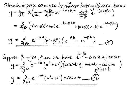
Note that, when we differentiate the step response to obtain the impulse response, the derivative without X has units of 1/s. But the input, X, is an impulse in units of V-s. When we multiply the derivative by X we obtain a quantity in V. Now let us integrate the response of the shaper circuit to see if it preserves the area of the pulse.
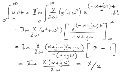
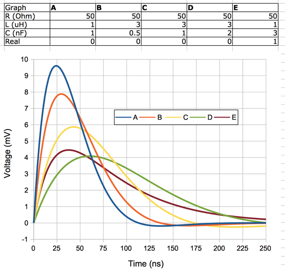
With no shaper, the area would also be X/2, by the action of the resistor divider made by the two resistors R. The shaper stretches out the pulse, but conserves its area. The Shaper sheet in our Filter Tool allows you do enter values for L, C, and R so as to obtain the theoretical output of the shaper to an impulse of area 1 V-ns. We obtain the following plots for a selection of values.
We constructed the following shaper using a metal box, two BNC sockets, a coil of wire, and a 1-nF ceramic capacitor.
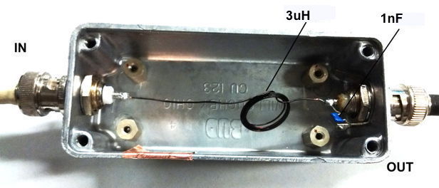
We measure the inductance of the coil using a resistor and a function generator before we install the coil in the shaper. Its inductance is roughly 3 μH. The capacitor is 1 nF. We connect a 50-Ω coaxial cable from the output to a 50-Ω terminated oscilloscope input set to 20 mV/div and 20 ns/div. We generate a 20-ns pulse and look at it with the same voltage and time scale. We deliver the pulse to a ×5 amplifier and then to the shaper, all with 50-Ω coaxial cable. The photograph below shows the pulse at the amplifier input, and the pulse at the shaper output.
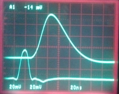
Calculated plot C corresponds to our component values 3 μH and 1 nF, and it peaks at 8 mV for a 1 V-ns input. The input pulse we see on the oscilloscope is not X, but rather X/2. Counting squares under the input pulse trace, we estimate its area is 1 V-ns, so the area of X is 2 V-ns. We expect the peak of y to be 16 mV. The output pulse on the oscilloscope is 5y, and its peak is 80 mV, so y is 16 mV, in good agreement with our calculation. We make another shaper with an 8-μH inductor and 2-nF capacitor.
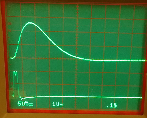
Our calculation suggests a pulse length of around 300 ns, which agrees well with the above measurement. For those of you who use Python, here is a pulse-shaper simulation script that generates a directory full of output pulse plots for a range of shaper component values: shaper_sim.py (by Xinfei Huang).
A SAW (surface acoustic wave) filter is a small, passive device made out of piezoelectric crystal. Most SAW filters are band-pass filters. The Demodulating Amplifier of the Octal Data Receiver A3027 uses a 915-MHz SAW band-pass filter to reject RF power outside the frequency range 930 MHz to 970 MHz. We describe our first use of a SAW filter here.
Take a thin, rectangular piece of piezoelectric crystal. Its top surface is flat. The crystal expands and contracts with applied electric field. If we tap the crystal, it will shiver for a short time, like a crystal wine glass, but at a frequency too high for us to hear. As the crystal shivers, it develops a voltage across its surfaces that matches the frequency and amplitude of the shiver. If we put electrodes on the top and bottom surface, the crystal will resonate when we apply a sinusoidal voltage of the correct frequency. Crystal oscillators use this resonance to create a frequency that is as accurate as the dimensions and flatness of the crystal.
A SAW filter does not use bulk resonance of a crystal. It uses surface acoustic waves. Instead of electrodes on opposite faces of a crystal, the SAW filter has two interlocking combs of electrodes on one end of the crystal surface, and another two such combs at the opposite end, but on the same crystal surface. We connect our input across these combs, as shown below.
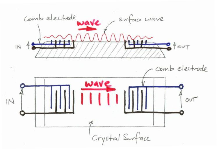
The combs set up electric fields along the surface of the crystal, instead within the bulk of the crystal. The electric fields cause the surface of the crystal to expand and contract. If we apply a sinusoidal voltage across the input electrodes of just the right frequency, we will create a surface wave that propagates across the crystal, where it creates a voltage across the output electrodes, which are also interlocking combs. You can see that only frequencies with a whole number of wavelengths between the teeth of each comb will be reinforced as they propagate across the comb fingers. The result is a filter: only frequencies that match the combs at both ends will be transformed from electrical signals into surface wave signals and back to electrical signals again.
Waves travel along the surface of the crystal at a velocity dictated by the crystal's Young's modulus, and is of order 4000 m/s for piezoelectric crystals. The wavelength of a 950-MHz wave propagating at this speed is only 4.2 μm. At such high frequencies, SAW filters tend to use harmonics of the fundamental resonant frequency of its combs. They do this by starting with a comb designed for an integer fraction of the desired band-pass frequency, and then inserting cuts in the comb fingers that make the combs inefficient at the fundamental frequency, but efficient at the desired band-pass frequency.
Let's compare the frequency response of the DSF947.5 SAW filter to that of polynomial filters.
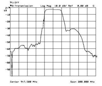
If we imagine that the SAW filter is a combination of a high-pass filter at the low end of its pass-band, and a low-pass filter at the high end, then we can compare its response at the high-end to that of a polynomial low-pass filter. We see that within 10 MHz of the cut-off frequency, the SAW filter's virtual low-pass filter response drops by 30 dB. Suppose we were to try to build a polynomial low-pass filter with the same response. A ten-pole 3-dB ripple Chebyshev filter response drops by 30 dB after a 10% change in frequency. In other words, the SAW filter cut-off at both ends of its pass-band is ten times sharper than of a ten-pole 3-dB ripple Chebyshev filter. Surface acoustic wave filters cost about $3 each and are available in 3-mm square packages.
A transmission line is a cable for carrying an electrical signal from one place to another. We usually don't think of transmission lines as filters, but they do provide some filter-like functions, and their behavior is interesting. We have a separate web page dedicated to transmission lines, Transmission Line Analysis. An imperfectly-terminated transmission line of finite length, called a transmission line stub, can be used to create an impedance for matching a source to a load, in place of a network of capacitors, inductors, and resistors, as we discuss in the Transmission Line Stubs section of our transmission line page.
We assemble the following circuit with a 100-μH inductor and a 100-pF capacitor.
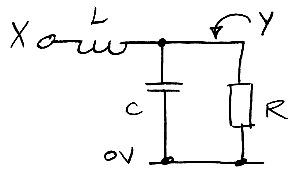
We try different values for the resistor, R. The oscilloscope screen shots below show the response of the circuit to a logarithmic sweep in frequency from 50 kHz to 5 MHz.
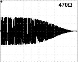
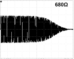
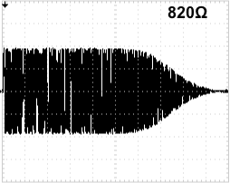
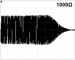
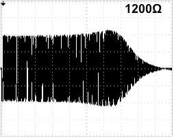
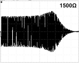
The response of our filter for 820 Ω looks like the maximally flat Butterworth response. Suppose that is our ideal, and we want to reproduce the filter on hundreds of circuits without adjusting the components for each circuit. A ± 10% variation in the resistance makes no significant difference in the response. We can use standard 5% resistors. The circuit is even less sensitive to the values of L and C. A 20% change in L or C in this circuit has the same effect as a 10% change in R. We can use standard 20% accurate capacitors and inductors. When we increase the number of poles in the filter, however, the accuracy we require of the components increases. When we change a single capacitor by 20% in a four-pole, passive, low-pass filter, its gain will change by 3 dB at some place in its pass-band. We need to use 5% capacitors and inductors if we want a four-pole passive filter to be accurate to better than ±1 dB. An eight-pole passive filter filter requires 2% accuracy in capacitors and inductors, and 1% for resistors. A 2% accurate capacitor costs ten times as much as a 20% accurate capacitor.
The demands upon capacitors in active filters are more severe: the location of the poles varies as the value of the capacitance, not the square root of the capacitance. High order active Butterworth filters do, however, remain practical: the value of RC for an active Butterworth filter is the same for every stage. We can use resistor and capacitor arrays to implement the RC values, and we will be sure that the values of RC will be within 1% of one another. Even if the absolute accuracy of the array resistance of capacitance is only 5%, we find that the variation within the array is less than one tenth of the absolute accuracy. We find the same relative-accuracy effect within a reel of surface-mount resistors or capacitors, so that the relative accuracy of a reel of 5% resistors will by 0.5%, and of a reel of 20% capacitors will be 2%. (We measured twenty resistors and capacitors from each of several reels before we made this claim.) The relative accuracy of surface-mount parts within the same reel makes active filter circuits more practical than they would be otherwise.
It will rarely matter if our active filter's cut-off frequency is moved by ±5% by component variation. It is more important that the relative position of the filter poles remains accurate, so that the poles work together to give the correct filter shape. A 5% variation in component values can re-arrange the poles of a Butterworth filter so as to introduce a 5-dB ripple in the pass-band. But we can build a Butterworth filter with flat response by using an array of resistors and capacitors for the common value of R and C in each stage, and by using 1% resistors in the voltage divider that determines the gain of each stage.
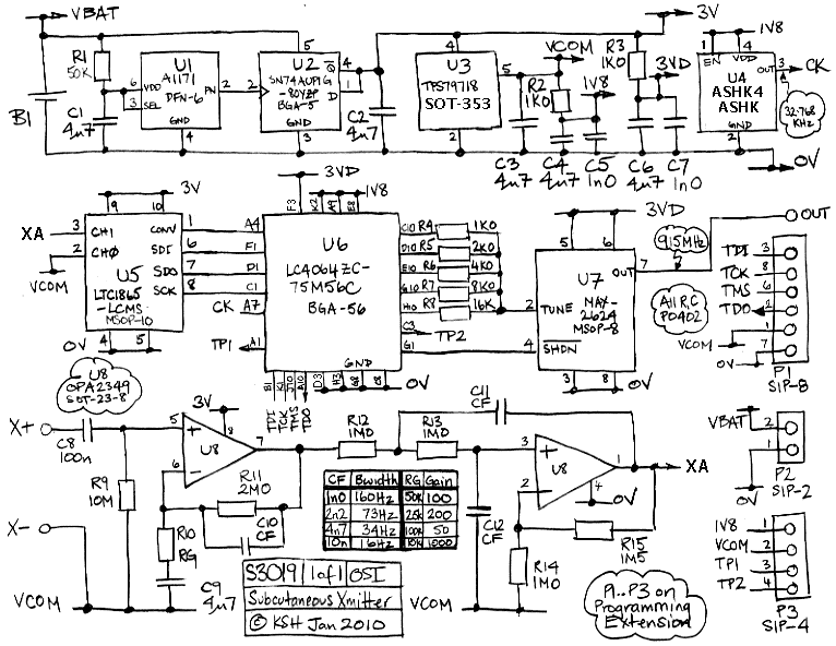
The same is not true for a Chebyshev filter, where each stage has a different value of RC. But we can still use an array of capacitors, so that all the capacitors are the same to within 1%, and then use 1% resistors, which are freely available and inexpensive. The figure below shows how the response of a three-pole 3-dB ripple Chebyshev low-pass filter varies from one assembled circuit to the next (for schematic see S3019).

The entire filter consists of the three-pole 160-Hz low-pass response plus a one-pole 1.7-Hz high-pass response. In the low-pass filter, we use 5% accurate capacitors of only one value, 1 nF, taken from the same reel for all circuits. The low-pass filter resistors are 1% accurate. Each value resistor comes from the same reel, but there are several values in the filter. The response from 10 Hz to 200 Hz varies by ±0.7 dB. The cut-off frequency of each filter is within a few Hertz of the designed value. The high-pass filter is made from a 5% resistor and a 10% capacitor. Its response from 1 Hz to 3 Hz varies by ±1.5 dB.
By using capacitors taken from the same reel, and relying upon precision resistors, we are able to produce a filter whose gain is known to within 0.7 dB within its pass band, and which produces a dramatic cut-off at a frequency within 3% of its designed value.