| Silkscreen Issues |
| VHDL |
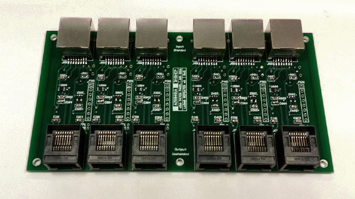
The A2084 is an updated version of the LWDAQ Repeater (A2058/A2059). It has the same six-connector layout and 140-mm length as the A2059. The width is increased from 56.5 mm to 75 mm. Per the LWDAQ Specification, the input sockets are shielded and the output sockets are unshielded.

The A2084 repeats logic signals by replicating the transmit circuit of a LWDAQ driver.
The metal shielded connector of the LWDAQ Repeater connects to the (upstream) LWDAQ Driver. The plastic unshielded connector connects to the (downstream) multiplexer or device. In this configuration, the LWDAQ Device can be used normally. Loop time will be increased by roughly 25 ns. In theory another repeater could be connected downstream, but we don't consider this possibility in design or testing.

To shut off downstream power to the device and/or multiplexer, send address word "0000" to the repeater. This can be accomplished by acquiring any instrument except the Dosimeter with device_mux_socket set to "0".
Note: All our schematics and Gerber files are distributed under the GNU General Public License.
S2084_1: SchematicThe A208401A and A208401B have a few component labels that are unreadable due to via placement. Those labels can be seen here.
[11-JAN-2016] We use two versions of our power supply switch on current generation of electronics. The first uses NDS355AN and NDS356AP MOSFETs as seen on the A2075; the second uses ZXTP2025F and ZXTN2031F BJTs and was developed for the nSW Bar Head (A2082). Preliminary work has shown a strong relationship between bias across the MOSFET oxide and vulnerability to ionizing radiation. The A2075-type switch has a 30V bias from the gate to the source of the P-channel MOSFET Q3 when the switch is off.
We have also investigated the effects of neutron damage on the gain of bipolar junction transistors. We observe a factor-of-five drop in gain after an exposure of 2*10^13 1-MeV neutrons ("20 Tn") in the ZXTP2025F and ZXTN2031F. We determine that the radiation exposure to the repeater in the nSW will be minimal due to its large distance from the beamline. However, we view the MOSFET damage as a potentially larger problem in general and elect to use the A2082-type power supply in the A2084.
[28-JUN-2016] We have the A208401A prototype printed circuit board. We cut the track that delivers 3V5 to pin 1 of the programming cable and replace it with a wire to 1V8.
[21-JUL-2016] We run our VHDL ring oscillator at 70 MHz. It draws 6 mA. We propagate the signal A to an output pin B. That signal is used to drive the LVDS output to the unshielded connector. We set the device power to be continually on (in lieu of an address receiver), and it draws ~12 mA from +15V and ~7 mA from -15V. With power provided, we operate a A2073 five-way switch and successfully take an image with a A2075 camera.
We take the loop time with the repeater and a one meter cable, and notice either a 25 or 50 ns increase. Given our measured cable delay of 10 ns/m, 20 of that is attributed to the cable. We attribute the variation in loop time to signal jitter. The signal edges vary by +/- 7 ns, which violates the LWDAQ Specification, but functions so far.
[27-JUL-2016] The "A" version of the A2084 lacks emitter resistors on the switches that control the two "WAKE" signals. Each switch draws roughly 70 mA when the pin on the LC4064ZE logic chip is set high. The voltage at the output of the pin is 0.7V rather than 3V. Shorting the base and emitter of the transistor only increases the current draw by 2 mA. So, the output of the logic chip is at its maximum. We solder 2.2kΩ resistors in between the emitter of the ransistor and ground on three of the six channels.
[09-JAN-2017] We have thus far been unable to get our VHDL LWDAQ Command Receiver to properly acknowledge address words on the LC4064ZE chip. Even when an address strobe is created, the downstream power remains up.
We take the ABEL code written for the A2075 and eliminate the asynchronous reset. We set pins 16 and 38 to toggle on the zero bit of the address word. The downstream power now toggles appropriately when we send a command to multiplexer socket "0" on the repeater. We take an image with an NBCAM, and see no problems. Ring oscillator period is 14 ns at a brisk 17.5°C. DA is delayed 110 ns, DDA 210 ns. Even though the repeater does not need to produce these signals, we would like the command receiver to meet spec, so we increase the dda_delay constant to 17. DDA is delayed by 225 ns. Loop time is 100 ns with a 3m cable from repeater to driver, and a 0.5m cable from repeater to BCAM.
[XX-APR-2017] We change the firmware of the A2084 to shut down the LVDS drivers when the downstream power is shut off.
[XX-MAY-2017] We find a repeater with two channels consuming 6 mA additional current in all states; the board remains functional. We replace the logic chip to no effect. We replace the LVDS chip and the problem goes away. We will test the current consumption of all channels before shipping.
[05-JUN-2017] We elect to proceed with production of the A2084 repeater code with ABEL firmware. The following is retained for future reference.
[21-JUL-2016] We struggled to replicate our ABEL ring oscillator in VHDL, due to the synthesis tool optimizing propagation delays out of the gate level design. Our initial strategy is to use an unused pin as a known logic low, and to use the logical construct "A NOR ZERO" to simulate "NOT A". The first version of the ring oscillator runs at period 20 ns with three gates and 33 ns with five gates. It draws 6 mA from +5V. We remove the counter that we previously used to divide the signal (to 40 and 60 ns, respectively). Without the counter the oscillator runs at 14 ns for three gates and 20 ns for five. It continues to draw 6 mA.
We have occasionally observed that the Synplify synthesis tools will vary the delay of a ring oscillator based on which outputs are routed to the test points. It appears that routing a signal to a test pin can occasionally cause it to be negated twice. In our ring oscillator we declare a signal and feed it to a NOR gate. If we then route that signal to a test pin, the synthesis tool will 1) create the negation of the signal, 2) feed it to an OR gate, 3) negate the signal again, 4) feed it to the output pin. We could perhaps avoid this by routing the negation of the signal to the pin. For now, we remove the test pin, and the oscillator frequency returns to normal.
When a 50 ns start bit is repeated, we notice variation in the signal length equal to the length of the ring oscillator clock cycle. We sample fifty 50-ns pulses on a variety of oscillator frequencies.
| # of gates | Clock Period (ns) | Short/Long (ns) | % of Short Pulses |
|---|---|---|---|
| 2 | 10 | 40/50 | 12% |
| 3 | 14 | 43/57 | 66% |
| 5 | 20 | 40/60 | 50% |
| 7 | 27 | 27/54 | 28% |
| 13 | 47 | 47/94 | 96% |
The jitter in the outgoing logic signal appears to be a result of the clock. The asymmetry of 43/57 may be a result of sample size. The LWDAQ Specification requires the signal edges to be accurate to +/- 5 ns.